Hi,
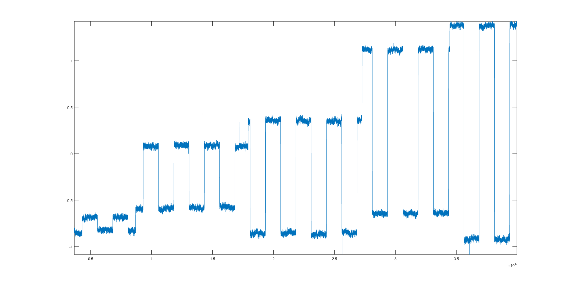
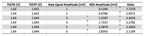
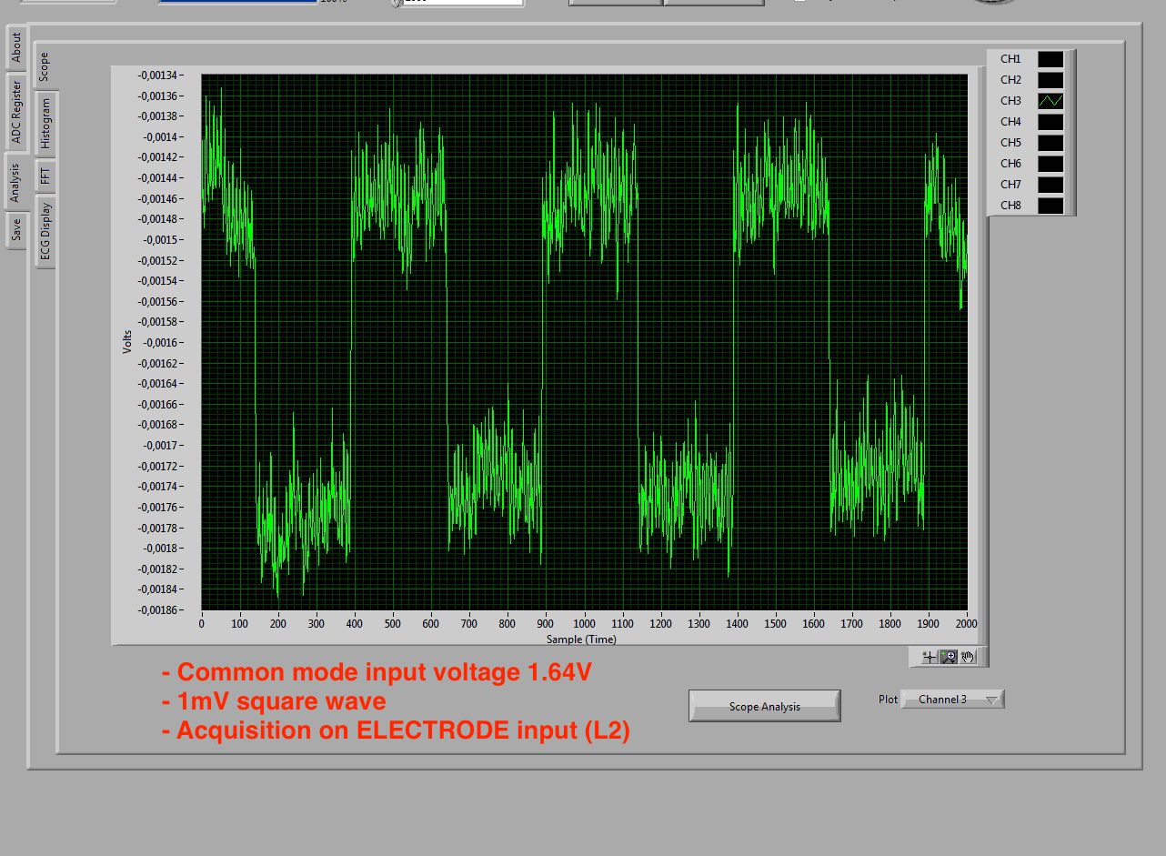
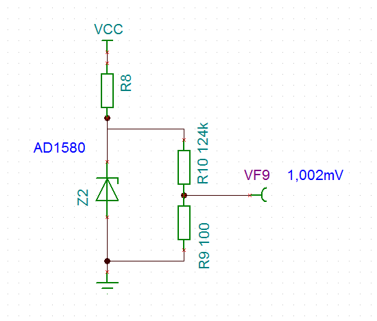
we would like to implement an external calibration within our 8-channels ECG device. The normative EN 60601-2-47 requires 1.0 ± 0.05 mV at the ECG inputs. To do so, we combined a high-precision voltage reference and a voltage divider with precision-type resistors. The circuit is able to provide the calibration signal of 1.0mV with the required accuracy.
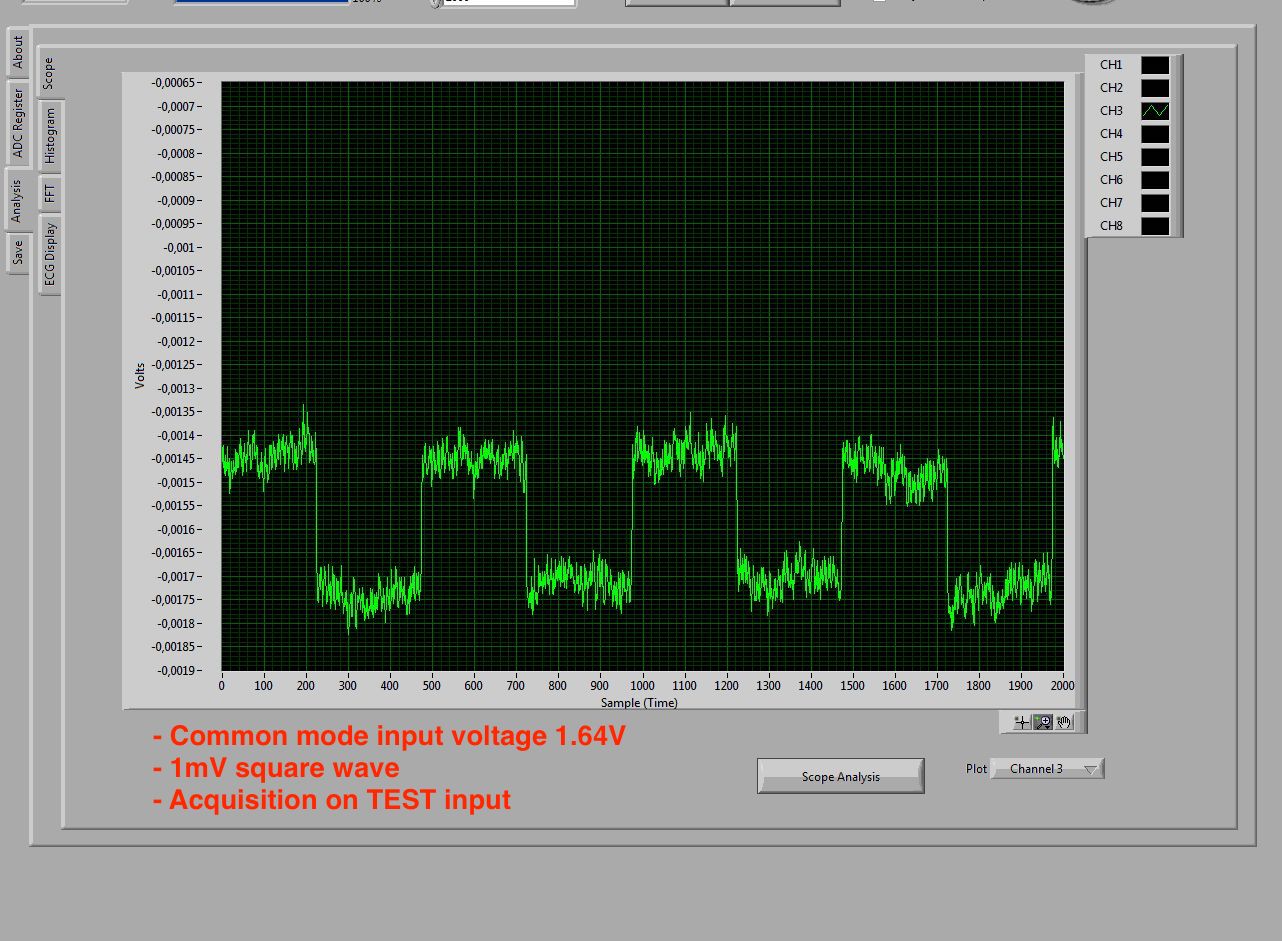
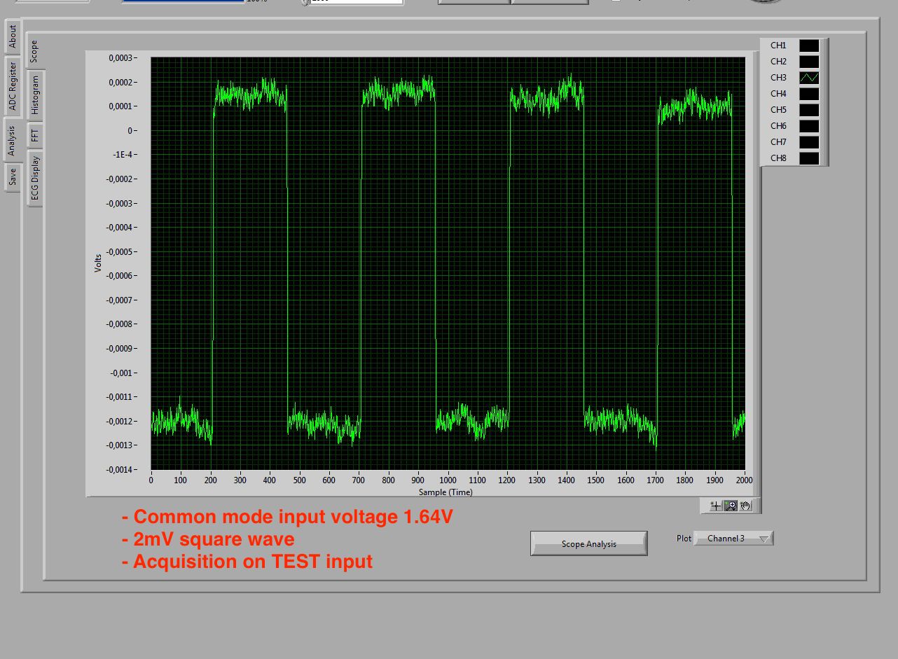
On the ADS1298, TESTN_PACE_OUT2 is connected to GND, while TESTP_PACE_OUT1 is muxed between the calibration signal and GND to create a step signal. The register of each channel is all set to TEST_SIGNAL while the test signal source of the CONFIG2 register is set to external.
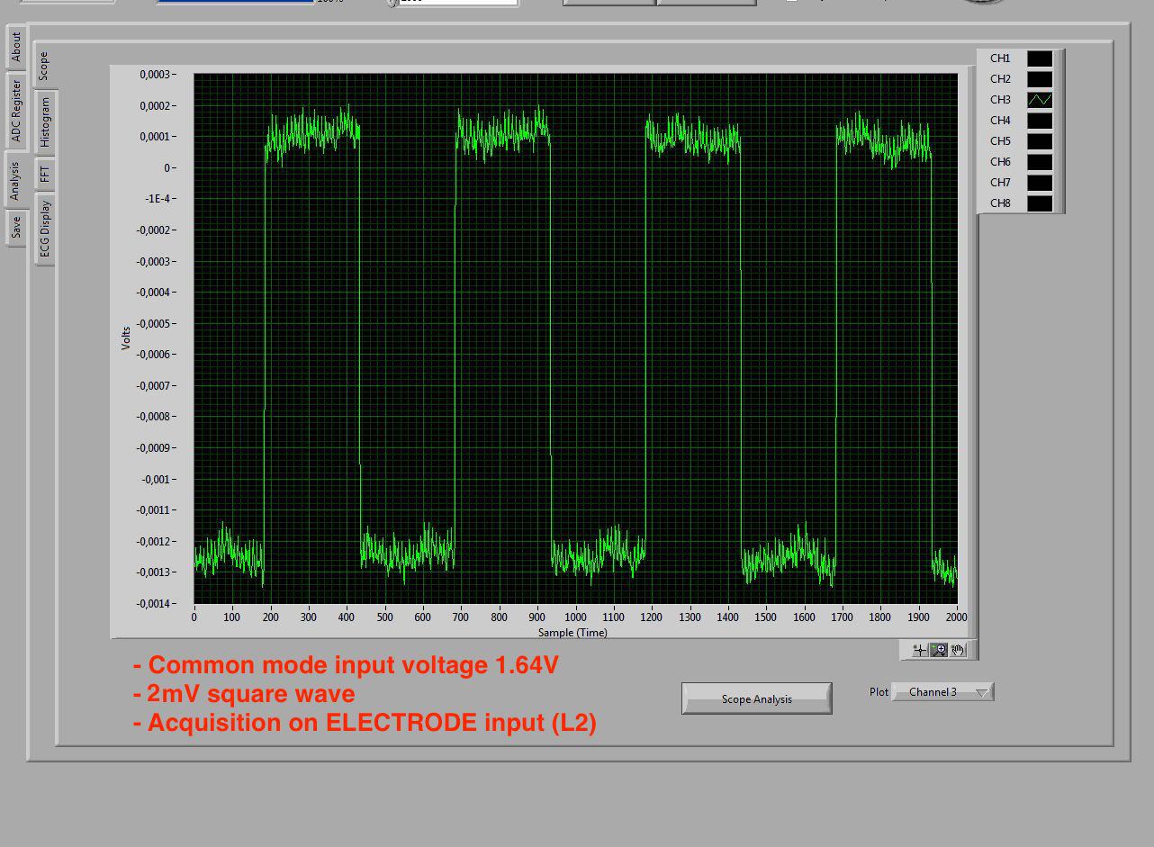
What we notice is that the ADS1298 seems not capable to distinguish the calibration signal level (1.0mV) from GND level (0V). However if we try to apply a calibration signal of 3mV (change the 100Ω resistor with a 300Ω resistor), we see a difference.
Are we missing something into the ADS1298 configuration? Could it be that the ADS1298 is not capable to acquire a DC signal at such a low voltage level? Is there any example application of the calibration of the ADS1298 using an external reference signal?
Thanks.
Regards,
void set_all_ads1298_reg (TADS1298REGS * all_reg)
{
    /*---------------------------------------*/
    /*config1 register*/
    /*---------------------------------------*/
    all_reg->config1.control_bit.reserved=0;
    all_reg->config1.control_bit.hr=HIGH_RESOLUTION;
    all_reg->config1.control_bit.daisyen=0;
    all_reg->config1.control_bit.clken=0;

    all_reg->config1.control_bit.rsv=0;

    all_reg->config1.control_bit.dr=HR_500SPS; //4KSPS
    /*---------------------------------------*/

    /*---------------------------------------*/
    /*config 2*/
    /*---------------------------------------*/
    all_reg->config2.control_bit.rsv7=0;
    all_reg->config2.control_bit.wct_chop=0;
    all_reg->config2.control_bit.inttest=0;
    all_reg->config2.control_bit.rsv3=0;
    all_reg->config2.control_bit.testamp=0;
    all_reg->config2.control_bit.testfreq=0b00;
    /*---------------------------------------*/

    /*---------------------------------------*/
    /*config 3*/
    /*---------------------------------------*/
    all_reg->config3.control_bit.pdbrefbuf=1;
    all_reg->config3.control_bit.rsv6=1;
    all_reg->config3.control_bit.vref4v=0;
    all_reg->config3.control_bit.rldmeas=0;
    all_reg->config3.control_bit.rldrefint=1;
    all_reg->config3.control_bit.pdbrld=1;
    all_reg->config3.control_bit.rldloffsens=0;
    all_reg->config3.control_bit.rldstat=0;
    /*---------------------------------------*/

    /*---------------------------------------*/
    /*LOFF*/
    /*---------------------------------------*/
    all_reg->loff.control_bit.compth=0b000;
    all_reg->loff.control_bit.vleadoffen=0;
    all_reg->loff.control_bit.ileadoff=0b00;
    all_reg->loff.control_bit.fleadoff=0b01;
    /*---------------------------------------*/

    /*---------------------------------------*/
    /*ch1set*/
    /*---------------------------------------*/
    all_reg->ch1set.control_bit.pd=0;
    all_reg->ch1set.control_bit.gain=GAIN_1;
    all_reg->ch1set.control_bit.rsv=0;
    all_reg->ch1set.control_bit.mux=INPUT_TEST_SIG;
    /*---------------------------------------*/

    /*---------------------------------------*/
    /*ch2set*/
    /*---------------------------------------*/
    all_reg->ch2set.control_bit.pd=0;
    all_reg->ch2set.control_bit.gain=GAIN_1;
    all_reg->ch2set.control_bit.rsv=0;
    all_reg->ch2set.control_bit.mux=INPUT_TEST_SIG;
    /*---------------------------------------*/

    /*---------------------------------------*/
    /*ch3set*/
    /*---------------------------------------*/
    all_reg->ch3set.control_bit.pd=0;
    all_reg->ch3set.control_bit.gain=GAIN_1;
    all_reg->ch3set.control_bit.rsv=0;
    all_reg->ch3set.control_bit.mux=INPUT_TEST_SIG;
    /*---------------------------------------*/

    /*---------------------------------------*/
    /*ch4set*/
    /*---------------------------------------*/
    all_reg->ch4set.control_bit.pd=0;
    all_reg->ch4set.control_bit.gain=GAIN_1;
    all_reg->ch4set.control_bit.rsv=0;
    all_reg->ch4set.control_bit.mux=INPUT_TEST_SIG;
    /*---------------------------------------*/

    /*---------------------------------------*/
    /*ch5set*/
    /*---------------------------------------*/
    all_reg->ch5set.control_bit.pd=0;
    all_reg->ch5set.control_bit.gain=GAIN_1;
    all_reg->ch5set.control_bit.rsv=0;
    all_reg->ch5set.control_bit.mux=INPUT_TEST_SIG;
    /*---------------------------------------*/

    /*---------------------------------------*/
    /*ch6set*/
    /*---------------------------------------*/
    all_reg->ch6set.control_bit.pd=0;
    all_reg->ch6set.control_bit.gain=GAIN_1;
    all_reg->ch6set.control_bit.rsv=0;
    all_reg->ch6set.control_bit.mux=INPUT_TEST_SIG;
    /*---------------------------------------*/

    /*---------------------------------------*/
    /*ch7set*/
    /*---------------------------------------*/
    all_reg->ch7set.control_bit.pd=0;
    all_reg->ch7set.control_bit.gain=GAIN_1;
    all_reg->ch7set.control_bit.rsv=0;
    all_reg->ch7set.control_bit.mux=INPUT_TEST_SIG;
    /*---------------------------------------*/

    /*---------------------------------------*/
    /*ch8set*/
    /*---------------------------------------*/
    all_reg->ch8set.control_bit.pd=0;
    all_reg->ch8set.control_bit.gain=GAIN_1;
    all_reg->ch8set.control_bit.rsv=0;
    all_reg->ch8set.control_bit.mux=INPUT_TEST_SIG;
    /*---------------------------------------*/

    /*---------------------------------------*/
    /*rld_sensp*/
    /*---------------------------------------*/
    all_reg->rldsensp.value=0;
    /*---------------------------------------*/

    /*---------------------------------------*/
    /*rld_sensn*/
    /*---------------------------------------*/
    all_reg->rldsensn.value=0;
    /*---------------------------------------*/

    /*---------------------------------------*/
    /*loff_sensp*/
    /*---------------------------------------*/
    all_reg->loffsensp.value=0x00;
    /*---------------------------------------*/

    /*---------------------------------------*/
    /*loff_sensn*/
    /*---------------------------------------*/
    all_reg->loffsensn.value=0x00;
    /*---------------------------------------*/

    /*---------------------------------------*/
    /*loff_flip*/
    /*---------------------------------------*/
    all_reg->loffflip.value=0x00;
    /*---------------------------------------*/

    /*---------------------------------------*/
    /*GPIO*/
    /*---------------------------------------*/
    all_reg->gpio.value=0x0F; //input
    /*---------------------------------------*/

    /*---------------------------------------*/
    /*PACE*/
    /*---------------------------------------*/
    all_reg->pace.control_bit.rsv=0b000;
    all_reg->pace.control_bit.pacee=0b00;
    all_reg->pace.control_bit.paceo=0b00;
    all_reg->pace.control_bit.pdpace=0;
    /*---------------------------------------*/
    /*---------------------------------------*/
    /*RESP*/
    /*---------------------------------------*/
    all_reg->resp.value=0x20;
    /*---------------------------------------*/

    /*---------------------------------------*/
    /*CONFIG4*/
    /*---------------------------------------*/
    all_reg->config4.control_bit.freq=0b000;
    all_reg->config4.control_bit.rsv4=0;
    all_reg->config4.control_bit.singleshot=0;
    all_reg->config4.control_bit.wcttorld=0;
    all_reg->config4.control_bit.pdbloffcomp=0;
    /*---------------------------------------*/

    /*---------------------------------------*/
    /*WCT1*/
    /*---------------------------------------*/
    all_reg->wct1.control_bit.avfch6=0;
    all_reg->wct1.control_bit.avlch5=0;
    all_reg->wct1.control_bit.avrch7=0;
    all_reg->wct1.control_bit.avrch4=0;
    all_reg->wct1.control_bit.pdwcta=1;
    all_reg->wct1.control_bit.wcta=0b010;
    /*---------------------------------------*/

    /*---------------------------------------*/
    /*WCT2*/
    /*---------------------------------------*/
    all_reg->wct2.control_bit.pdwctc=1;
    all_reg->wct2.control_bit.pdwctb=1;
    all_reg->wct2.control_bit.wctb=0b100;
    all_reg->wct2.control_bit.wctc=0b011;
    /*---------------------------------------*/

    return;
}