This thread has been locked.

If you have a related question, please click the "Ask a related question" button in the top right corner. The newly created question will be automatically linked to this question.

TSW54J60EVM: TSW54J60EVM: clock to FPGA

Part Number: TSW54J60EVM
Other Parts Discussed in Thread: LMK04828, ADS54J60, , SN65LVDS4

Hello Team,

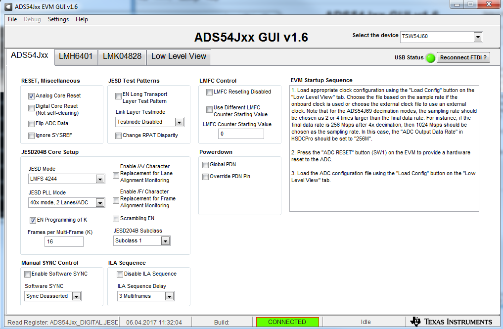
I am using two TSW54J6EVM with one Xilinx Zynq UltraScale+ XCZU9EG-2FFVC900IES. Therefore I designed a PCB to connect the two TSW54J60 FMC´s with the Zynq UltraScale+. I want to use the "to FPGA" pins of the TSW54J60´s to supply the Xilinx IP-Core´s with the clock from the LMK04828. I use the ADS54JXX  EVM GUI to set the ADS54J60 with LMFS = 4244 and to set the LMK04828 for the ADC und FPGA frequenzy. There are the following config files to set the frequenz:

122.88 MHz, 245.76 MHz, 307.2 MHz, 409.6 MHz, 450.56 MHz, 491.52 MHz, 614.4 MHz, 819.2 MHz, 983.04 MHz and 1024 MHz.

 I know the the lanerate with the ADC config is ADC_frequenz * 10. But can you tell me the to FPGA speed for these configurations?


Best Regards

Tobias

  • Hello Team,

    if I use the LMK_Config_Onboard_122p88_MSPS file and set my JESD204 IP-Core to a line rate of 1.2288 Gbps and the reference clock (which is connected with the to FPGA pins) to 122.88 MHz the code group synchronisation between ADC and FPGA works. I only tested this because I see that the DCLK Divider of CLKout 0 /1 (FPGA Clock & SYSREF) and CLKout 2/3 (ADC Clock & SYSREF) are both set to 20. Can you please tell me how the to FPGA clock speed for the rest of the config files is?
    I have another question: I actually use the ADS54J60_LMF_4244 file with LMK_Config_Onboard_122p88_MSPS. The JESD204 IP-Core from Xilinx has an debug status register. If I read this I can see that all lanes has code group sync, start of ILA was detected and lane is currently receiving K28.5's. But the start of data bit is never set. It seems something is going wrong in the ILA sequenz and the ADS54J60 still sends K28.5's. The IP-Core only recognize the start of the ILA sequenz but it seems that the ADS54J60 didn´t send his configuration octets (second Multiframe of the ILA sequenz). The IP-Core has some register to save the configuration octets and they are empty. Maybe someone can help me what I am doing wrong and why the ADC didn't send user data?

    Best Regards
    Tobias
  • Tobias,

    Are you using the TSW14J10EVM to interface to the Xilinx board? What Xilinx board are you using? If you are running the firmware from TI, the clock rates for the FPGA calculations are shown in the attached User's Guide on page 15. For your other question, if the ADC is still sending K28.5 characters, the link never entered the ILA sequence. The FPGA is still holding SYNC low I am guessing. Can you verify this?

    Regards,

    Jim

     1261.SLAU580B.pdf

  • Hello Jim,

    thanks for the attached User´s Guide. I don´t use the TSW14J10EVM. I use the Xilinx Zynq UltraScale+ XCZU9EG-2FFVC900IES FPGA (link: shop.trenz-electronic.de/.../TE0808-03-02I-UltraSOM-Zynq-UltraScale-Modul-2-GByte-DDR4-20-x-serielle-Transceiver ) with UltraITX+ Basisboard (Link: shop.trenz-electronic.de/.../TEBF0808-04-UltraITX-Basisboard-fuer-Trenz-Electronic-TE0808-UltraSOM ). This configuration is like the Xilinx Zynq UltraScale+ MPSoC ZCU102 (Link: www.xilinx.com/.../ek-u1-zcu102-es2-g.html ). The ADC musst entering the ILA sequenz. If i use the Link Layer Testmode Constant K28.5 the register of the IP-Core shows: Lane is currently receiving K28.5's and Lane has Code Group Sync. So all is correct. If I disable the testmode or use the repeating ILA mode the register value patterns but meanly shows: Lane is currently receiving K28.5's, Lane has Code Group Sync and Start of ILA was Detected. The IP-Core detects the start of ILA so the ADC musst at least sent a R character.

    Regards
    Tobias
  • Hello Jim,

    I used a oscilloscope to measure the SYNC signal on "SJP3 SYNC_SEL" pin 2. If I use the testmode "constant K28.5" the SYNC signal on pin 2 is permanent high. So the ADC gets the SYNC signal from FPGA. If I disable testmode the SYNC signal switches between high and low. So the ADC does something in the ILA sequenz wrong and the FPGA set the SYNC signal low. Do you have some other ideas which? Is there something else I can measure to give you more information? I see in the config file ADS54J60_LMF_4244 that the parameter K is set to 16. Is that the correct value? Here are my settings with the GUI

    Regards,

    Tobias

  • Tobias,

    There is a register write missing in this configuration file. Please copy the attached file and replace the existing one located at:

    C:\Program Files (86)\Texas Instruments\ADS54Jxx EVM GUI\Configuration Files

    Regards,

    JimADS54J60_LMF_4244.cfg

  • Dear Jim,

    thanks for your supply. I used the new config file but I get the same result. I only get with testmode constant K28.5 a stable SYNC Signal. I measured the to FPGA clock on capacitor C79 with a oscilloscope. It´s about 125 MHz so looks ok. I also measured the SYSREF signal on resistor R38. This looks strange and I am not sure if it´s "normal". See here:

    Maybe the SYSREF signal from the LMK04828 is the problem?

    Regards,

    Tobias

  • Hello all,

    I am using the recently released Rev. H of ADS54JXX EVM GUI (April 7th, 2017) now. I see this thread: e2e.ti.com/.../588897.    Can you tell me when a stable version of the ADS54JXX EVM GUI will be released of how to fix this problem? Furthermore can someone help with the problem above which is still not answered? Is it possible thate the SYSREF signal from the LMK04828 is the problem or maybe the second multiframe from the ADS54J60?

    RRegards

    Tobias

  • Tobias,

    The GUI is fine as long as you only use the provided configuration files. Are you using the TSW14J56EVM to test this board? The SYSREF signal is turned off by the configuration file after the ADC has been configured. That is why you are seeing this. Please send me the two configuration files you are loading the TSW54J60 with. Do you press the reset button on the TSW54J60EVM after loading the LMK config file and before loading the ADC config file?

    Regards,

    Jim

  • Jim,

    thank you for your post. I know that the GUI runs with the configuration files. I use the ADS54J60_LMF_4244.cfg file and a modified version where I set the register 0x690002 to 0x40 to enable K28.5 pattern. So its a litte circular to use for every setting a seperate config file. I still use the same FPGA as desribed to you above.I always press the reset button on the TSW54J60EVM after loading the LMK config file before loading the ADC config file. Here are the two configuration files I load to the TSW54J60EVM:2477.ADS54J60_LMF_4244.cfgLMK_Config_Onboard_122p88_MSPS.cfg

    Regards,

    Tobias

  • Tobias,

    Xilinx has a way to ignore ILA errors. Please enable this and see if SYNC stays stable and valid data is captured by the FPGA. Is the Zync board expecting SYSREF as LVDS? Is it going to the correct pins between the FMC and FPGA? Do you have a TSW14J56EVM to double check the TSW54J60EVM?

    Jim  

  • Jim,


    can you tell me where the option for ingoring ILA errors is? I can´t find this in the documentation. Yes, the Zync board expect the SYSREF as LVDS and I checked the pins for correct connection. I don´t have a TSW14J56EVM. But I have two of the TSW54J56EVM so I don´t think there is a bug on the board.

    Regards

    Tobias

  • Tobias,

    I cannot answer your question. I am guessing the error is related to a read of an invalid checksum, which is the 13th octet of the link configuration data.  I would check the Xilinx JESD document, that can found from the following link:

    https://www.xilinx.com/support/documentation/ip_documentation/jesd204/v7_1/pg066-jesd204.pdf

     I also suggest you contact your local Xilinx support for more help regarding this.

    Regards,


    Jim

  • Jim,

    I know this document and read it several times while my implementation. I can´t find the option to disable the ILAS on the IP-Core. I only know this option in the ADS54JXX GUI. I added a integrated logic analyzer in my VIVADO design and analyse the data from the PHY IP-Core to the RX IP-Core. Here is a screenshot when the error happens:

    You can see in the gt0_rxdata[31:0] that first "bcbcbcbc" characters ar incoming for CGS. This is stable for long time.To start the first multiframe of the ILA sequenz the ADS54J60 musst send a R-character which has a 8-bit value: 00011100 and in hex: 1C. There is an 1C in the first data block after the bcbcbcbc block. But as you can see there are 11*32 Bit blocks between the first bcbcbcbc and the last bcbcbcbc which signalize the restart of the CGS. 11*32bit = 352 bit => 44 octets. In my configuration I use K = 16 and F = 4 => a multiframe consists of 64 octets. So the error happens in the first multiframe of the ILA sequenz. I hope this can help you a little.

    Regards

    Tobias

  • Tobias,

    Is the SYNC signal that is going to the ADC set to the proper logic level? It appears to me the ADC is never seeing SYNC go back high and stay high. Is there a way to manually control this signal with your FPGA? We do not have this issue with any of our platforms (both Altera and Xilinx). Is the power supply you are using for the TSW54J60m rated for at least 3 Amps? Is the PLL Lock2 LED on after you configure the LMK on this board? Do you issue a board level reset after loading the LMK and before loading the ADC? Can you send me the actual config files you are loading? There was an error with one of them in an earlier release of the ADC GUI. Just want to make sure you are not using this file.

    Regards,

    Jim  

  • Jim,


    I use the differential SYNC at pin G12 and G13 on the FMC which goes to the SN65LVDS4. I didn´t change the SJP3 SYNC_SEL so if I measure at pin 2 of SJP3 SYNC_SEL it looks like this:

    As you can see there is a SYNC signal on pin 2 of SJP3 SYNC_SEL which is connected to the SYNC pin of the ADS54J60. So the ADC musst get the SYNC from FPGA. The high time of the SYNC is variable but sometimes it is about 200 ns like the last one in the picture.

    The power supply I use can deliver 5 A. After I load the LMK04828 config file the PLL lock2 LED is on and I do the ADC reset before I load the ADS54J60 config file. Here are both config files I use:

    7142.ADS54J60_LMF_4244.cfg 5584.LMK_Config_Onboard_122p88_MSPS.cfg

    I hope this infos can help you.

    Regards,

    Tobias

  • Tobias,

    The first octet of a multiframe is always 0x1C and the last octet is 0x7C. In your data shown above, the multiframe is 16 fames or 64 octets. In the ILAS standard, the link configuration data does not occur until the second octet of the second multiframe. This is indicated by a 0x9C, which I never see above. Your system is not even getting to this stage as the SYNC drops out and the BCBC data starts appearing again. I am guessing the K value is not matching between the two parts as it appears the FPGA might be expecting the link configuration data before the ADC is ready to send it, thus causing the FPGA to reset SYNC.

    Regards,

    Jim

  • Jim,

    I know that the error happens in the first multiframe of the ILAS and told you in my post on Apr 27, 2017 8:07 AM (see above). I guess this problem is caused by the ADS54J60. I built a JESD204B data generator in VHDL which sends the data like the TSW54J60EVM should. The data generator sends K-chars and after a SYNC signal from the IP-Core he sends the 4 multiframes for ILAS. In the second multiframe he sends R-char, Q-char, the 14 configuration-octets and A-char .There didn´t happen any error and the IP-Core stores the configuration data from the data generator in his register space and send the testsamples from the data generator with a tvalid signal. So the IP-Core works correct.

    Regards,

    Tobias

  • Tobias,

    Make sure your RBD value is equal to or less than K. What value are you currently using? Your test VHDL cannot possible simulate the entire TSW54J60 link interface as you are not using the actual FMC connection. There are many other things you cannot simulate but I will not go into this. This board works fine with both our Altera and Xilinx platforms. Did you try using less lanes, a smaller K, a slower sample rate? I have a feeling there is a just a parameter or two that is off.  I had a customer that had a similar problem and the fix was to change his RBD value to one that was less than K.

    Regards,

    Jim