A related question is a question created from another question. When the related question is created, it will be automatically linked to the original question.
If you have a related question, please click the "Ask a related question" button in the top right corner. The newly created question will be automatically linked to this question.
Thanks for your interest in our ADS127L01. Unfortunately, we do not have firmware source code that we can send to you. If you have specific questions about using the interface, please let me know and I can help you with that.
for(i = 20; i>0; i--); // Add time between transmissions to // make sure slave can process information while (!(UCA1IFG&UCTXIFG)); // USCI_A0 TX buffer ready? UCA1TXBUF = 0x42; // OFC0 for(i = 20; i>0; i--); // Add time between transmissions to while (!(UCA1IFG&UCTXIFG)); // USCI_A0 TX buffer ready? UCA1TXBUF = 0x01; // OFC0 for(i = 20; i>0; i--); // Add time between transmissions to while (!(UCA1IFG&UCTXIFG)); // USCI_A0 TX buffer ready? UCA1TXBUF = 0x55; // OFC0 for(i = 20; i>0; i--); // Add time between transmissions to while (!(UCA1IFG&UCTXIFG)); // USCI_A0 TX buffer ready? UCA1TXBUF = 0xAA; // OFC0
for(i = 20; i>0; i--); // Add time between transmissions to // make sure slave can process information while (!(UCA1IFG&UCTXIFG)); // USCI_A0 TX buffer ready? UCA1TXBUF = MST_Data1; // Transmit first character
for(i = 20; i>0; i--); // Add time between transmissions to // make sure slave can process information
while (!(UCA1IFG&UCTXIFG)); // USCI_A0 TX buffer ready? UCA1TXBUF = MST_Data2; // Transmit first character
for(i = 20; i>0; i--); // Add time between transmissions to
P1OUT |= 0x80; // A2D CS high for(i = 20; i>0; i--); // Add time between transmissions to
__bis_SR_register(LPM0_bits + GIE); // CPU off, enable interrupts }
switch(__even_in_range(UCA1IV,4)) { case 0: break; // Vector 0 - no interrupt case 2: // Vector 2 - RXIFG P1OUT &= ~0x80; // A2D CS low
while (!(UCA1IFG&UCTXIFG)); // USCI_A0 TX buffer ready? A2D_data1 = UCA1RXBUF; UCA1TXBUF = 0x0; // Send next value
for(i = 20; i>0; i--); // Add time between transmissions to // make sure slave can process information while (!(UCA1IFG&UCTXIFG)); // USCI_A0 TX buffer ready? A2D_data2 = UCA1RXBUF; UCA1TXBUF = 0x0; // Send next value
for(i = 20; i>0; i--); // Add time between transmissions to // make sure slave can process information while (!(UCA1IFG&UCTXIFG)); // USCI_A0 TX buffer ready? A2D_data3 = UCA1RXBUF; UCA1TXBUF = 0x0; // Send next value
for(i = 20; i>0; i--); // Add time between transmissions to // make sure slave can process information while (!(UCA1IFG&UCTXIFG)); // USCI_A0 TX buffer ready? A2D_data4 = UCA1RXBUF; UCA1TXBUF = 0x0; // Send next value
for(i = 20; i>0; i--); // Add time between transmissions to // make sure slave can process information while (!(UCA1IFG&UCTXIFG)); // USCI_A0 TX buffer ready? A2D_data5 = UCA1RXBUF; UCA1TXBUF = 0x0; // Send next value
for(i = 20; i>0; i--); // Add time between transmissions to // make sure slave can process information while (!(UCA1IFG&UCTXIFG)); // USCI_A0 TX buffer ready? A2D_data6 = UCA1RXBUF; UCA1TXBUF = 0x0; // Send next value
for(i = 20; i>0; i--); // Add time between transmissions to // make sure slave can process information while (!(UCA1IFG&UCTXIFG)); // USCI_A0 TX buffer ready? A2D_data7 = UCA1RXBUF; UCA1TXBUF = 0x0; // Send next value
for(i = 20; i>0; i--); // Add time between transmissions to // make sure slave can process information while (!(UCA1IFG&UCTXIFG)); // USCI_A0 TX buffer ready? A2D_data8 = UCA1RXBUF; UCA1TXBUF = 0x0; // Send next value
for(i = 20; i>0; i--); // Add time between transmissions to // make sure slave can process information P1OUT |= 0x80; // A2D CS high
for(i = 20; i>0; i--); // Add time between transmissions to // make sure slave can process information break; case 4: break; // Vector 4 - TXIFG default: break; } }
It is very difficult for us to read through a portion of someone's code and fully understand the problem. The easiest way for us to verify the interface is by looking at a scope capture of the ADS127L01 SPI signals from a logic analyzer. These would include SCLK, DIN, DOUT, /DRDY, /CS, and CLK.
Before trying to read/write to the ADS127L01, I would suggest verifying that all supplies and clock signals are present as expected. As long as you are sending the master clock (CLK) and START is pulled high, you should notice that the /DRDY pin is toggling at the output data rate. This indicates that the ADC is converting and outputting new data. Have you verified this yet?
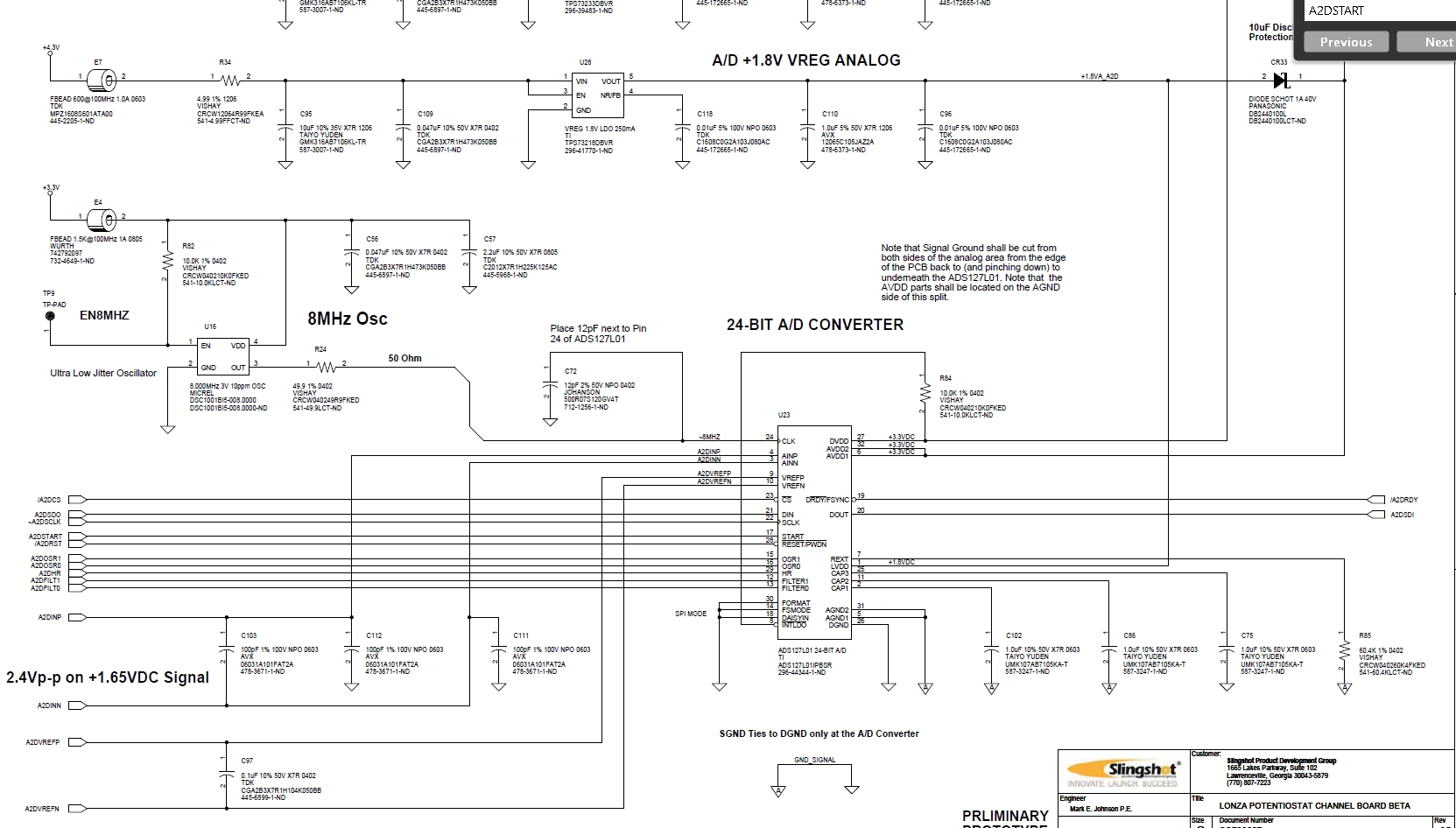
Please provide the configuration of all Hardware Mode Pins on your ADS127L01 as well as the supply voltages and clock input frequency. If you'd like, I can review your schematic.
Yes, I have verified all the pins on the chip are at expected levels. Also verified that /DRDY is toggling high once every 4 usec, for about 250nsec whenever the START pin is high.
Schematic attached.
The problem I'm having is that I'm just doing a simple read of the 8 registers, expecting to read the same data every time. Instead I usually get all zeros, and sometimes other random data. I never see the ID register with a 0x3 in the lower nibble as expected.
The schematic and pin settings look ok. Are you still having an issue with this? Please share a logic analyzer scope capture of the register read command. Make sure to at least show SCLK, /CS, DIN, DOUT, and CLK.