This thread has been locked.

If you have a related question, please click the "Ask a related question" button in the top right corner. The newly created question will be automatically linked to this question.

Two ADS1282s don't synchronized

Other Parts Discussed in Thread: ADS1282

Hi,everyone,I have a problem about ADS1282 asking for help.Thank you.

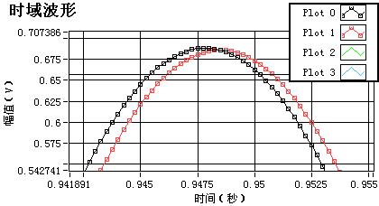
Two ADS1282s don't synchronized.Figure 1 shows that channel 2(red) is delayed than Channel 1(white).On the oscillograph,Figure 2

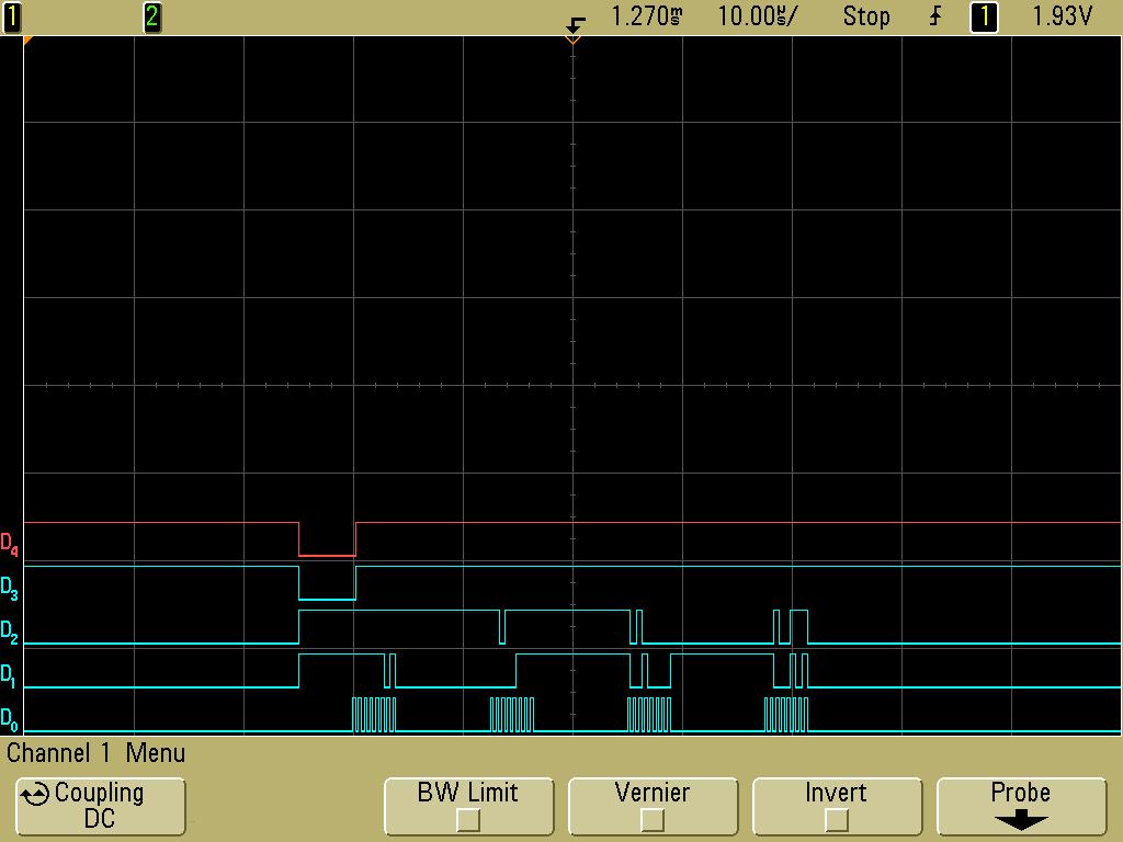
shows that the DRDYn was coinstantaneous,but the data from two ADS1282 per samping were not same.On my PCB,the two ADS1282s' SYNC

pin was connected.And I take the SYNC pins low and then high to synchronize the two ADS1282s before collecting the output data.So

where the problem lies?

  • Figure 2

    from up to down there are:DRDY2, DRDY1, Dout2, Dout1, SCLK

  • Zhuo,


    Offhand, I'm not sure of anything that could cause the behavior you describe. It almost appears that the delay is almost three tdata long from device to device. I will note that the ADS1282 is a fairly complicated part so I'll need a lot more information

    First, with respect to Figure 1, you have two curves showing signals that are offset in time.
    1. Is this the measurement from the ADC for the two devices?

    2. What is the input source that you are measuring?

    3. What is the input frequency?

    4. How is the ADS1282 configured (gain, data rate, everything)?

    5. Do you have the raw data (hex code) that comes out of the ADC? If the codes are converted to voltage, there might be some conversion error and I like to read through the data directly from the ADC.

    6. Have you changed the input to something different? Different magnitudes, frequencies or even using a DC signal migh show something.


    Second, Figure 2 shows the DRDYn signal and then the clocking out of data. It looks like the DRDYn signals are aligned together so that the devices are some how synchronized, even if the data appears to be offset in time as in Figure 1. I still had a few questions though.

    1. Have you tried measuring the input voltage with the scope to see if there really is some sort of lag between the two signals.

    2. If I read the data correctly, it looks like the first ADC reads FFDFA027h and the second ADC reads FD079005h. If the reference is 5V, then the full scale is +/-2.5V and this data corresponds to approximately -2.5mV for the first and -58mV for the second. This roughly corresponds to what you show in Figure 1, but I might be nice to see a few more scope shots to see if that is real.


    Finally, it might be nice to get a schematic for your circuit. If it is proprietary, maybe a rough sketch of your system, including sources might help explain to me what you are measuring.


    Joseph Wu

  • HI Wu,

    I'll show more details.

    About Figure1:
    1. Is this the measurement from the ADC for the two devices?
    Yes,the Data is from the Dout pin(pin 4) of ADS1282s.

    2. What is the input source that you are measuring?
    The input is from Agilent Waveform Generator 33220A.The inputs of the two ADS1282s is the same(connected).

    3. What is the input frequency?
    20Hz,1400mVpp

    4. How is the ADS1282 configured (gain, data rate, everything)?
    CONFIG0  "01100010" that means 4000SPS others config is default
    CONFIG1  "00001000" all default
    HPF,OFC,FSC all default
    didn't calibration(OFC and FSC registers keep default)

    5. Do you have the raw data (hex code) that comes out of the ADC? If the codes are converted to voltage, there might be some conversion error and I like to read through the data directly from the ADC.
    I read through the data directly from the ADC

    6. Have you changed the input to something different? Different magnitudes, frequencies or even using a DC signal migh show something.
    I tried several sine waveform.The delay always existed.Otherwise,I tried DC sigenal and the waveform is Figure 3.A almost stable error between the two ADS1282.But obviously this stable error can not cause delay.


    About Figure2:
    1. Have you tried measuring the input voltage with the scope to see if there really is some sort of lag between the two signals.
    The two input is the same signal(Figure 4).

    2. If I read the data correctly, it looks like the first ADC reads FFDFA027h and the second ADC reads FD079005h. If the reference is 5V, then the full scale is +/-2.5V and this data corresponds to approximately -2.5mV for the first and -58mV for the second. This roughly corresponds to what you show in Figure 1, but I might be nice to see a few more scope shots to see if that is real.
    You are right.I'll show you a more full scope shot(Figure 4).

    Otherwise:
    1.comparing the waveform of 1000SPS and 4000SPS.I find out that the delay between the two ADS1282s is a constant,about 0.6ms.
    2.My progrmme is:
    ResetADS1282(reset pin low and the high)---->WiterRegister(CONFIG0 and CONFIG1)---->RDATAC Command---->SychronizeADS1282(SYNC pin low and the high)---->wait for more than 1ms(alt_busy_sleep(100000))---->Collecting DATA(begin when DRDY get low)---->Save DATA---->Show the Waveform
    3.The two ADS1282's registers were written at the same time.

    4.In my  circuit,the SYNC pins of  the two ADS1282s is connected togeteher.So as the Reset pins,PWDN pins,CLK pins and SCLK pins.

  • Figure 4: waveform in 1000SPS and 4000SPS

  • Zhuo,


    Thanks for the information. I'll continue looking this over and let you know if I have any questions.

    One thought that I had was that this might be a problem related to the filter in the ADS1282. Since there are many adjustable parts to the filter, it might create a different response to the measurement if the filters are not set to exactly the same thing.

    For example, the ADS1282 has a high-pass filter stage. If you look at Figures 50 and 51, you can see the gain and the phase response. At 20Hz this filter has some small phase delay and some small attenuation (as you see in your plots). This HPF stage can be used or bypassed. One thing to check is to vary the frequency and see if the phase delay gets worse at 1Hz inputs or if it goes away a 100Hz inputs. You can plot those inputs and see if the plots match up or get better with the change with frequency.

    Also, it might be important to try to read back all registers to make sure the configurations are the same.


    Joseph Wu

  • Zhuo,


    One other possibility would be external filter mismatches. If you have some sort of capacitive input filtering, the mismatches of the input capacitance or resistances may create a difference in the phase delay depending on the values.

    You can also see this if you vary your input frequency.


    Joseph Wu

  • Hi,Wu

    First of all,Thank you for your help.I'm very puzzled that I find the delay disappeared after I have reconnected the signal input wire.So I guess I had make a mistake in the connecting of signal input. In the origin one,the sig- of the two channel was connected to two GND separately.In the last one,the two sig- were connected together to one GND. May be the GND cause a delay. But it's strange that I can't recur the delay any more.

    After all,the problem was solved. But the reason is to be found.

    By the way,I have another two questions about the calibration of ADS1282:

    1.About OFSCAL command: You know,a stable zero input signal must be applied to ADS1282 before OFSCAL. I want to know where the stable zero input signal come from on a PCB?Is there another DA needed?

    1.About GANCAL command: You know,a stable  input signal must be applied to ADS1282 before OFSCAL. I want to know whether the input must be +fullscale or -fullscale?If it is,where the stable fullscale input signal come from on a PCB?Is there another DA needed? If is not,the ADS1282 dosen't know the Expected Code,how to calibration(equltion 13 on page 32 of datasheet).

  • Zhou,


    The calibration commands are used to adjust the measurements of the ADC so that the offset and gain error of the entire system can calibrated. However, in these commands, the user needs to be able to be able to switch in a 0V signal for the offset calibation and a full-scale input for the full-scale calibration.

    1. For the OFSCAL, the input can be shorted together and measured. This would be the offset of the system and can be either the input of the ADC or the input of the entire system. This offset should be in the center of the input range to eliminate the effect of any common-mode error. Once this offset is calculated, it is subtracted from subsequent conversions to eliminate the offset.

    2. First, note that you want to perform the oFSCAL before the GANCAL. This eliminates the offset from the full-scale calibration. Typically a GANCAL command is issued to calibrate a reference to the full-scale. When running this command, you want to input a positive full-scale value to the inputs. This then adjusts the ADC so that this positive full-scale voltage will give an output code that is full-scale. This essentially corrects for any gain error.


    Joseph Wu

  • Wu,

      Thank you for you help.I have learned a lot from your reply about calibration of ADS1282.But I still have a question.Usually,how did you make the psitive full-scale?I want to use the ADS1282 on my data aquiring PCB.What's the best way to supply the psitive full-scale signal on the board?

     That's all.It's very kind of you.I remembered that you have helped me many many times on this forum.Thank you very much.And anywhere I could make a help for you,I 'll do my best!

      Best wishes!

  • Zhuo,


    On your board, you have some reference set up for the ADS1282. This is connected to the VREFP and VREFN pins of the ADC. Often, this is set to 5V (or some buffered version of +2.5V to -2.5V.

    Ideally, output code = (full-scale code)*(analog input)*(2*PGA)/VREF

    However, this equation can be in error because of offset and the gain error. In the offset, we can remove the same code for every conversion to remove an offset error.

    For the gain error, this output code can be scaled slightly (to adjust for gain error in the ADC, or for gain error to the reference input). The calibration can remove gain error by setting the full-scale code to be equal to the full-scale voltage.

    One possible way this could be generated would be by creating a a precise voltage divider to get 1/2 of VREFP-VREFN. Another way is to measure a known precision 2.5V reference. There are many ways that this could be done, depending on how you have your system set up.


    Joseph Wu