This thread has been locked.

If you have a related question, please click the "Ask a related question" button in the top right corner. The newly created question will be automatically linked to this question.

ADS1120: external Vref = 2.5V when AVDD = 2.5V also

Part Number: ADS1120

Team-

We have an application of the ADS1120 where an external reference voltage of 2.5V is used while AVDD = 2.5V as well.

This appears to be within the recommended data sheet parameters, as shown below:
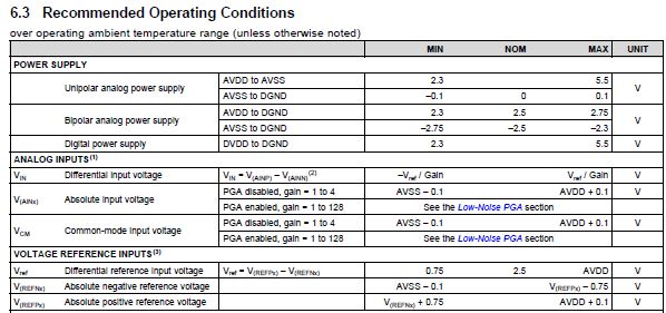
Section 8.3.6, page 29, states that "...all references inputs are internally buffered ti increase input impedance."

When operating at the rail, i.e. VREF = AVDD = 2.5V, will there be any addtional offset drift, or other non-ideal behavior that we should watch out for?

If not, why not?  It seems like internally it would be very difficult to buffer VREF as it's impossible to drive all the way to the AVDD rail?

Thanks, Best, S. Dunbar, AFA Colorado

  • Hi Steve,

    The  reference buffer for the ADS1120 is a precharge buffer as opposed to an op amp buffer.  The action of the switched capacitor input stage will periodically sample the reference.  The reference will charge an internal sampling cap.  The charge/discharge of the cap will draw current and an average current can derive an impedance.  Altering the cap value can affect the impedance as differing values of charge moving to and from the cap can be seen.  If during a portion of the sampling cycle the cap is precharged, then the amount of charge required from the reference source will be reduced and thus raising the impedance of the sampling circuit.

    The action of the precharge buffer is taken into account with the design, so you should not see any offset drift or non-linearity due to the precharge buffer itself.  You can kind of think of the buffer more like a switch that charges the cap for a short period of time then opens and connects to the reference. 

    Best regards,

    Bob B

  • Bob-

    Thanks for the response; the data sheet describes the reference pins as "buffered".
    I don't quite understand how the operation you described is buffered- what is the buffering mechanism between the external Vref pins and the sampling capacitor?

    From what you describe, it seems like we will still need to pay good attention to the properties of the external reference amplifier?

    Thanks, Best, Steve
  • Hi Steve,

    To some degree it is true that you should consider the reference driving source, however as is shown on page 7 of the electrical characteristics table the reference  input current is typically 10nA.  The ADS1120 is designed to use a resistor established reference (such as might be used in an RTD ratiometric measurement) using one of the IDAC sources.  So the input impedance is quite large.

    As far as the term 'buffer' there are many different types and construction.  In this particular case it is a precharge buffer.  A definition of the word buffer is to "lessen or moderate the impact of (something)".  If this were a static DC case the average current draw would be zero once the cap is charged and the impedance infinite. 

    In the precharge state, the reference input becomes isolated (buffered) and no current is drawn from the reference source.  Current to precharge the reference sampling cap comes from the analog supply.  It is the difference in current from the precharge state to the fully charged state that determines the impedance and lessens the impact of the reference sampling.

    Best regards,

    Bob B

  • Hi Bob,
    I'm the engineer at Keysight who asked Steve the question initially. Should I add additional bypassing on the reference pins to source the average current, and reduce any ripple? If so, how much capacitance on the reference pins is recommended? The EVM shows a 0.1uF between REFp0 and REFn0. I am driving the reference on many (48) ADCs from a common source, and I am considering adding a buffer on some of them, maybe one buffer for every 6 ADCs to avoid any loading effects. I was thinking about adding 10 ohm resistor in series with each one, and a 0.1uF across the reference pins, but I'm not sure if this would be a good idea or not. Would you have any concerns driving 48 reference inputs from a common reference source? Is there a buffer that could handle heavy capacitive loading that you would recommend that also won't add errors due to the op-amp offset drift?
    Thanks,
    Ben Hoover
  • Hi Ben,

    Welcome to the forum!  Yes, it would be a good idea to add a 0.1uF cap across the reference input pins and it would be ok to add a little filtering as well as you are driving so many ADCs and the potential for noise pickup would probably be high.

    Using a buffer is a good consideration but I don't think it would be required depending on the drive capability of the reference.  Questions regarding op amps would be better served by asking on the precision amplifier forum.  You would need to consider any offset and drift relative to the AVDD supply.  The maximum reference input is AVDD+0.1V.  You need to consider both the reference voltage stability as well as the AVDD supply stability to ensure good results.

    Have you considered using the AVDD supply as the reference?  This may simplify the approach as there is an internal reference connection to the AVDD supply in the ADS1120.

    Best regards,

    Bob B