Other Parts Discussed in Thread: DAC5652, DAC5672,
I'm working on a device that contains several DACs. I want conect several DACs to one bus, and use apart WRT(IQ) and CLK(QI) input. I have questions about managing the DAC.
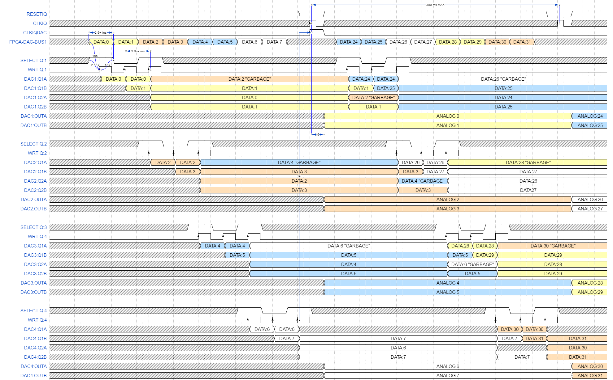
1) In the datasheet it is written that after setting the data on the bus D[11:0], I must set the "WRT" control signal and after the rising edge of the signal, I should wait for time tlat = 4 clk for "Clock latency (WRTA/B to outputs)". What is the time tlat? What "outputs" by meant? And what is meant by these 4 clk? Time equivalent to four frequency periods? What frequency WRT1 or CLK?
Or to set the values in the latch, I have to generate 4 pulses WRT or CLK?
I found PDF document "DAC5652, DAC5662 and DAC5672 Interleaved Data Mode" with filename "X2_Interleaved_Mode.pdf". In it document nothing written about 4 clk.
2) In the datasheet it is written that after setting the data on the bus D[11:0], in Dual-Bus mode, I must set the "WRT" control signal to tlph=2ns. What about this time in Single-Bus mode?
3) In the Single-Bus mode, the CLKIQ frequency is divided by 2 and then go to the DAC latch. What is it done for? What could connect two inputs CLK & WRT?
P.S. Sorry for my English =(
Thanks a lot, with best wishes, Nikita Alisov.