This thread has been locked.

If you have a related question, please click the "Ask a related question" button in the top right corner. The newly created question will be automatically linked to this question.

ADS8339: Strange input pin offset

Part Number: ADS8339
Other Parts Discussed in Thread: OPA227, OPA333, OPA320, INA117, THS4281, OPA2227

Hello,

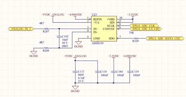
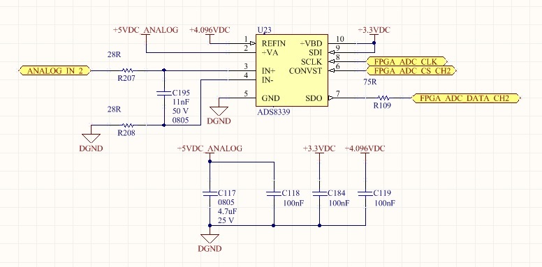
Below is a partial circuit schematic of a circuit using an ADS8339 ADC.

The analog_in_2 net is from an external source referenced to the same DGND. If this external source is disconnected, the analog_in_2 point floats at about 2.4V relative to DGND.

I do not understand how this 2.4V is generated.  It appears it is being sourced by the input pin.

If I connect analog_in_2 to an opamp outputting 0V, referenced to the same ground, the 2.4V disappears but the ADC measurement is nowhere near 0V, instead varying between 1190 to 1300 counts. 

Can someone from TI give me some suggestions as to what cause this behavior with this part?  Something with the layout or voltage reference?  I have used other TI ADCs like the 12 bit ADS7822U without issue.

Thanks!

  • Hello Brian,


    For some reason, the schematic does not display in the post above.  Please include in the schematic the ADS8339 input driver circuit and RC filter at the inputs, the reference driver circuit, supply connections and bypass capacitors for the device.


    Many Thanks and Best Regards,

    Luis

  • What is with this site and uploading pics?  Even paste from word didn't work:

    ADS8339 with RC filter input, bypass caps and supply connections:

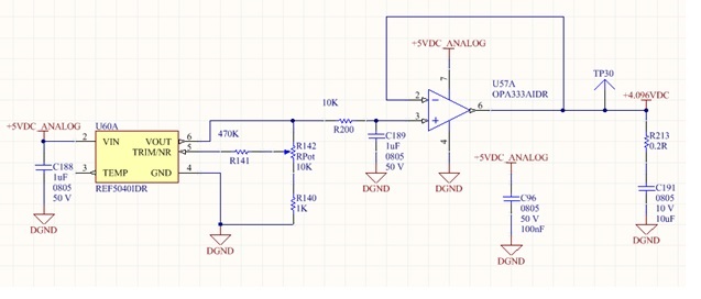
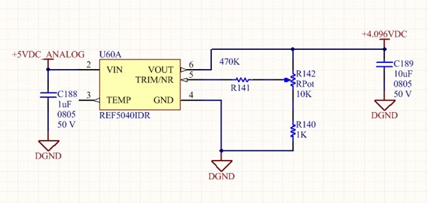
    I've tried a couple of different reference driver circuits with the same result.  Here is the first one:

    And the second attempt:

    This is the input circuit.  With this connected the IN+ pin reads zero, but the digital reading is around 1300 counts.  With the ANALOG_IN_2 net left floating, the net sits at about 2.4V relative to DGND.

    Thanks!

  • Hi Brian,

    Thank you for posting the schematic. I will be performing a couple of simulations to optimize the driver circuit and will also provide suggestions for the reference driver circuit.

    I expect to get back to you within the next couple of days,

    Thank you and Best regards,
    Luis
  • Thanks very much I appreciate it.  I'll keep watching the thread.

  • Hi Brian,

    I performed TINA simulations assuming a 250kSPS sampling rate:

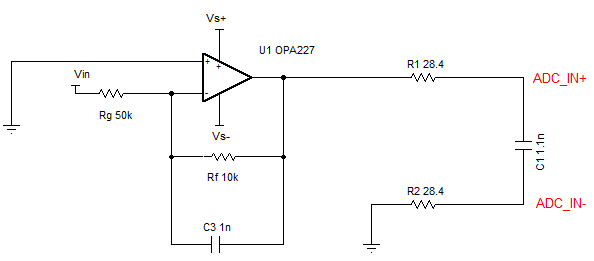
    -          The RC filter in front of the OPA227 is not optimal and therefore the amplifier driver circuit does not settle within the 700ns minimum acquisition time of the ADS8339. Please replace the RC filter with 28.4Ω+1.1nF+28.4Ω as shown below. This revised circuit will settle within the 700ns of the ADS8339. Please see attached the TINA transient simulation.

    Tina Simulation:

    OPA227_ADS8339_transient.TSC


    --          The OPA333 buffer is not capable of driving the REFIN pin of the ADS8339. The reference pin of a SAR ADC presents a dynamic load where the reference voltage is sampled several times during each conversion. Since the OPA333 is a has limited bandwidth, it is not able to recharge the reference bypass capacitor between conversions, and the reference voltage will droop. A suggestion is to replace theOPA333 with the OPA320 (20MHz BW). Please see attached REF5040+OPA320 simulation.

    REF5050_ADS8339_opa320.TSC

    -         Alternatively, the REF5040 without the buffer will be able to drive the REFIN pin of the ADS8339 directly without issues; although the reference will have a small droop error ~129uV (2 LSBs) during the first few conversions due to the transient response of the REF5040. If you use the REF5040 with the OPA320 as a buffer this will eliminate any reference droop error.

    Questions/Suggestions:

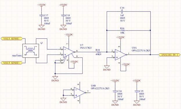
    -          The OPA227 requires the ±15V dual supplies. Although the device is set up as an attenuator, it may be possible that the device produces momentary signals above +5V or below GND during power up/power down or during any fault condition; exceeding the absolute max ratings of the ADS8339 and potentially damaging the ADC.  One possible suggestion is to add a protection clamp at the input of the ADS8339.   Alternatively, you could consider replacing the OPA227 with a single supply +5V amplifier circuit. Since the OPA is configured in the inverting configuration as an attenuator, it will handle the signals from the INA117.

    -          If available, we will be happy to review the PCB layout gerber plots/board layout as well.

    Please let me know if the issue persists after replacing the RC filter in front of the OPA227.

    Thanks and Regards,
    Luis

  • Hi Luis,

    Your suggested changes to the RC input filter have made a significant improvement.  Here is the new schematic (using the closest RC values I had available).

    Also note my sampling rate is currently set to only 12.5 KHz.  Is there more optimal RC values for different sampling rates that I could calculate?

    With an input of 2.048V I see a digital conversion output of 8000 hex, +/- about 60 counts, which is about what I would expect.

    Neglecting issues related to layout, are there any changes I could make on the schematic level to improve the accuracy, or generally design this better?  Reproducing my current ADC reference circuit below:

    I think the small droop error you mention when driving the reference pin of ADS8339 directly with REF5040 as shown here is not an issue for me, as the first several hundred samples will be ignored anyways.  The 10uF capacitor is currently a Murata X5R GSM series part which looks to have an ESR of 1 ohm or less at 20 KHz or greater.

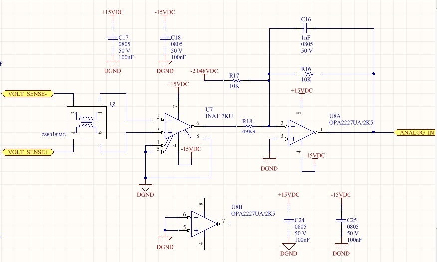
    In regards to the INA117/OPA227 circuit, I can't change to a single supply amplifier because my input can be both positive OR negative.  In other words, the voltage at INA117 pin 6 can be anywhere from +10 to -10V.  This is the circuit:

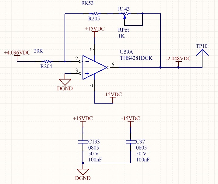
    This is how the -2.048V is generated.  I think I omitted this section earlier as I didn't not have it connected yet.

    Aside from the protection clamp which I will add, is there anything else I might change to optimize performance?

    Thanks again,

    Brian

  • Hi Brian,

    I apologize for the delay in the response.

    The  THS4281 is a high bandwidth amplifier (90MHz), and the maximum voltage across the negative and positive voltage supply is a unipolar 16.5V or bipolar +/- 8.25V.

    The amplifier at this node is not required to be very high bandwidth as it is connected to the non-inverting input of the opa2227 through a 10kOhm resistor.  Since you require a bipolar +/-15V supply in this application, and require to generate a -2.048V at the output of the inverting amplifier, a suggestion is to replace with an OPA227; this will give you better noise performance as well. 

    Please let me know if you have any questions,

    Thank you and Best Regards,

    Luis