This thread has been locked.

If you have a related question, please click the "Ask a related question" button in the top right corner. The newly created question will be automatically linked to this question.

ADS1271: Signal conversion range using pseudo differential configuration

Part Number: ADS1271
Other Parts Discussed in Thread: OPA350

Hi

Im using ADS1271 to digitalize an EMG signal.

The signal is supposed to go from 0 to 5V before entering the ADS. The problem is that when retrieving the data from the MCU, if the signal has a lot of peaks, the retrieved data looks noisy. Below is the signal seen on the oscilloscope and then the Matlab figure with the data seen by the MCU (this was with a medium force contraction)

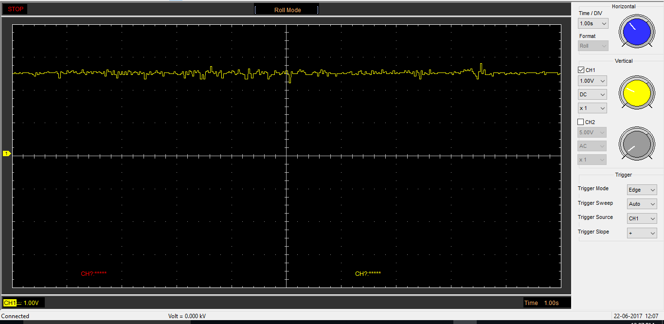
Here is a figure of the oscilloscope of an EMG data with a low force contraction: 

As you can see, when the signal has a higher amplitude or higher peaks, there are some samples quite outside the average range...

Below is the configuration used (High resolution and pseudo-differential configuration with AINN at 2.5V)

What could be the reason of that behavior? Or what can I do to correct this? Im concerned this could modify the signal frequency (the FFT results)... 

Is there a way to mmmm correct this with the MCU??

I attach also an image of Matlab with a high force contraction:

Thanks!!! 

  • Hola Miguel,

    The maximum differential input must be limited to +/-VREF (2.5 V in your application). It appears that at times, your differential input voltage exceeds 2.5 V, even 3 V, according to the MATLAB plots you show. Is the y-scale correct on the MATLAB plots?

    A couple questions just to clarify the measurement setup:

    1. It looks like your oscilloscope captures show an input signal centered around 2 V. Is this measured with respect to GND or with respect to AINN?
    2. Can you confirm that AINN is fixed to 2.5 V (also with respect to GND)? If AINP is truly between 1 V and 3 V, and AINN = 2.5 V, then the differential voltage should be between -1.5 V and +0.5 V. This is an acceptable input range that would not cause such behavior in the ADC.

    Best Regards,

  • Hi Ryan

    The data seen in Matlab is the data after being converted.  The scales is right, yes.

    1)The oscilloscope captures are centered on two for a problem Im having with the last opamp. For some reason, when incrementing the gain of the amplifier, the offset voltage drops. 

    2)AINN is indeed fixed at 2.5V (I checked it some weeks ago). AINP is supposed to go from 0 to 5V, as the ADS1271 is supposed to change from 0-5 to 0-3.3

    I attach the schematic of the filtering stage

  • Hi Miguel,

    In the first question, I was asking how the scope measurement was made. I assume the GND lead on the scope probe was connected to GND? So the DC common-mode voltage is about 2 V on AINP. Can you do the same measurement on AINN? From the MATLAB data, it appears that you have an average of 3 V between AINP and AINN, but according to your schematic, the differential voltage should be centered closer to 0 V.

    Best Regards,
  • Hi Ryan

    respecting the first question, yes. It was done with the GND pin and it is in fact close to 2V. 

    Also the AINN is at 2.5V. I just checked it again and is in fact at the correct voltage...

    Ryan Andrews said:
    but according to your schematic, the differential voltage should be centered closer to 0 V

    I guess you're right... The REFP is at 2.5 and the AINN is at 2.5 as we discussed some time ago to have a full scale on the conversion, from 0 to 5 V 

    Best regards

  • Exactly - so if AINP is centered around 2 V and AINN is around 2.5 V, I would expect the differential plots in Matlab to be around -500 mV. Instead they are close to 3 V, which is beyond the ADC full-scale. Let me know the result of measuring AINN. You could also measure AINP and AINN on the scope together and use the MATH function to plot the difference.

    Best Regards,
  • Hi Ryan

    I just ploted the difference (A-B). Here is the result.

    When measuring both signals, I saw that if the AINN was in 0, the red signal was equal to the yellow signal and then it would be using the full scale no? But in this post:  you told me to use the AINN at the same voltage as the reference to get full scale. Or Im missing something here? Is the comparison with the REFP? 

    Best regards

  • Hi Miguel - the comparison is with the differential reference voltage: REFP - REFN. You are correct that, if AINN = 0V and AINP goes from 0V to 5V, the differential input voltage will also go from 0V to 5V. This is not acceptable since your reference voltage is only 2.5V. This limits the differential input voltage range from -2.5V to +2.5V (not 0V to +5V).

    The (A-B) plot on the scope looks correct - that's exactly what I expected to see. The common-mode input voltage is about 2V - 2.5V = -500mV. Why does this not match the MATLAB plots? The differential input voltage (i.e. the "red" curve) is what the ADC is converting.

    Can you please zoom in on the CH1, CH2, and MATH curves on the scope and check the peak amplitude? You need to make sure that MATH function never exceeds +/- VREF (-2.5V to +2.5V). Over-driving a delta-sigma modulator (especially a high-order modulator like the ADS1271) can cause the modulator to saturate. This may explain the large transients you see in the MATLAB data plots.

    Best Regards,

  • Here is the signal with the measurement from the cursor to the lower peak

    Here is the same image but with the cursor in the middle of the signal

    The signal has an amplitude of ~3.3V. If the signal is measure from the middle, it shows a 1.85V... 

    Thanks

  • I see the issue:

    AINP (CH1) ranges from 0V to +3.5V
    AINN (CH2) is fixed at +3.25V

    The differential input voltage (MATH) ranges from -3.25V to +0.25V. You are exceeding the negative full-scale range (-2.5V). This is likely causing the modulator to saturate, which triggers an internal reset and produces the large transients shown in the MATLAB plots.

    Reduce the dc voltage on AINN to 2V. The differential input voltage range will then be -2V to +1.5V and will not cause this issue.

    Best Regards,
  • How could AINN be fixed at 3.25 if the pin is connected to the REFP at 2.5??

    I saw a problem Im having with the amplification stage, which is moving the signal below 0 before the last stage (the offset stage).

    I tried using a function generator and didn't have that problem... not that I recall

    Look: this signal was a sine at 30Hz

    Could this be caused by the filtering stage?? 

    Regards =)

  • Hi Ryan
    Hope you'r doing great.
    Apparently there is a problem with the signal conditioning but Im looking to solve it =)
  • Hi Ryan

    Hope you're doing great

    I was trying to figure this out but haven't ben successful and was wondering... could this be caused by the pseudodifferential configuration of the ADS1271? because this only occurs when Im using a lot of force to generate the signal but not when Im applying low force. I was thinking that this could be because of the difference between the signal and the AINN and VREFP is quite big. Because I tried even with a small amplification, where the signal was far away of the voltage limits and it kept happening... 

    Or could there be other reason?

    EDIT:

    I saw that the lower peaks are not constant in length. The peaks vary a lot and that the lower part corresponds to the signal. look:

    it looks like a jump of the signal but it should be continuos but it has a low jump of 1 sample. and the ~10 samples at the bottom correspond to the upper part of thee signal. Nevertheless, if I add 3.25 to that samples, the signal goes back to "normal": 

    Nevertheless i did some tests with other signals i had recorded and mmm well lets say that was not the solution... but i already ran out of ideas... 

    Thanks!

  • Hi Ryan. Hope you're doing great.
    I answer the post but I didn't receive any mail so I wrote this to see if I get one now
  • Hi Miguel,

    I assume the blue curve is the ADC output, but how did you acquire the orange curve? Is this the same set of data? Please explain the difference between the two curves.

    If the y-axis is plotted in Volts, then we still have the same issue as before. As I described in my posts on May 17th, the modulator may saturate and reset if you apply a differential input voltage that is greater than the reference voltage. The duration of these pulses corresponds to the amount of time that the overvoltage condition is present.

    I recommend replacing the electrode inputs with a function generator for now. Use a fixed sine wave frequency (say 100Hz) and slowly increase the amplitude. Monitor the output voltage of your signal conditioning stage on AINP as well as the differential voltage between AINP and AINN. Compare this to the ADC output. That should indicate exactly which conditions are causing this issue.


    Best Regards,

  • Hi Ryan

    Ryan Andrews said:
    I assume the blue curve is the ADC output, but how did you acquire the orange curve? Is this the same set of data? Please explain the difference between the two curves.

    If the sample was below 0.5, then I add 3.25. like sampleX+3.25

    Ryan Andrews said:
    I recommend replacing the electrode inputs with a function generator for now. Use a fixed sine wave frequency (say 100Hz) and slowly increase the amplitude. Monitor the output voltage of your signal conditioning stage on AINP as well as the differential voltage between AINP and AINN. Compare this to the ADC output. That should indicate exactly which conditions are causing this issue.

    okok. This could be the amplitude of the signal and could be solved by reducing it right? I will perform some tests tomorrow since today Im quite tight on time and that tests take a lot of time to be able to pass the information to Matlab to plot it. 

    Thanks!

  • Ryan
    This just came into my mind...
    Even when the signal cannot go beyond 0 to 5V, Im having an offset problem with the analog filtering. The signal is not centered at 2.5V as supposed because the Notch filters adds a negative offset on the signal and with the amplification this offsets increases. So the problem is on the filtering, not on the ADC. Check the images of this post: e2e.ti.com/.../2194448
    the ones from the oscilloscope
  • Hi Ryan

    Hope you're great

    I just did some tests. Even with a super low amplification:

    the problem persisted.... 

    Here is the Math line:

    All the channels are on 1V/div

    I don't know whats going on.... The Oscilloscope doesn't show any problem but the ADS always digitalize the signal that way... 

  • Hi Ryan

    Hope you're great

    I was wondering if you had any idea of what could be going on...

    Thanks!

  • Hi Miguel - have you tried replacing the voltage on AINN with a separate 2.5V source? In other words, do not short VREFP and AINN together. Does this give a different result?

    Also, could you please share the raw data from the ADC? I can accept either decimal or hexadecimal format, preferably in an Excel or text file if you can. Thanks!

    Regards,

  • I dont know... the board is already dine and the components are already there...

  • I share you the data:

    test_data.zip

    If you plot the data on Matlab, you will find that the data gets cut at 3.25V and the rest of the signal, which is around 5V at the end, is in the lower part. The slope of 1sample is like if the signal was converted but with a different venter value. You can change the 'prueba2.csv' to the other 'pueba_1xlb_x' without problem. The files with 'prueba' are with the first filters and the 'data_filters.csv' is with the new filters, completely centered at 2.5V. It looks like if the signal was divided into two sections... 

    I also share you the lines of matlab I used to fix the data:

    original_data=csvread('prueba2.csv');
    average=0;
    for i=1:4155
    
        if data>1.65 % EDITED ORIGINALLY 0.5
            original_data1([i])=original_data([i])-3.3;
        else
            original_data1([i])=original_data([i]);
        end
        
    end
    average=average/4155;
    figure
    plot(original_data)
    hold on
    plot(original_data1)
    title('prueba 15lb 1')

    Best regards

  • Thank you, Miguel. I will try to take a look at this today.

    I would still suggest trying the other test with AINN and REFP separated. I understand you will have to make some modifications, but it may tell us something. Do you have at least one board you can "sacrifice" and blue-wire a separate 2.5-V to AINN?

    Best Regards,

  • I have not the tools for that. And another problem is that the paths are in the inner layers...
  • Is the data in volts? I would like to see the raw data in hexadecimal or decimal format please.
  • is in decimal format in volts yes
  • By raw data, I mean the actual ADC output codes (i.e. 0x7FFFFF or 8,388,607 is the ADC full-scale output code to represent 2.5V). Can you share the data this way instead?
  • Miguel - I also tried to simulate the reference buffer - it is not stable. During the ADC sampling, both the reference pins and input pins are sampled by an internal switched-capacitor sampling circuit. Each internal sampling circuit draws an instantaneous amount of current, which produces a voltage transient on those pins that needs to settle between conversions.

    Since the reference buffer configuration is not stable, it will not be able to respond very well to these transients. Please revise the OPA350 circuit as recommended below.

    The closed-loop frequency response below shows significant gain peaking, which is a sign of an unstable circuit with inadequate phase margin:

  • Ryan Andrews said:
    By raw data, I mean the actual ADC output codes (i.e. 0x7FFFFF or 8,388,607 is the ADC full-scale output code to represent 2.5V). Can you share the data this way instead?

    I have not the data in that format and also there is a problem...

    The MCU SPI has a 16bit buffer (configurable to be less) and Im using two transmissions of 12 bits each. Then I concatenate them. The problem here is that the results of the conversion I can only watch them once they are in the MCU.

    What I don't get is why, when using a signal generator I have no problems at all. When I used the new filters design in a prototype board I hot this result:

    If the VREF signal was behaving in an unstable manner, as you described, I would expect that every signal I introduce to the ADS1271 was converted as the image above but no... or am I wrong? And also... the configuration used is the suggested diagram on the Datasheet...  

    If you look closer to the plots on matlab, you will see that the data looks cut if the signal is above 3.25V and the peaks are placed close to 0...

    You told me that it could be the amplitude of the signal. Nevertheless, even when I changed it to a minimum possible value for the signal to be seen, the behavior was the same... But only if the signal was recorded when performing a stronger contraction on the muscle. This behavior occurred even with the new filters...

    What could be happening?

    Best regards

  • Hi Ryan

    I share you two figures:

    The image of the left is the signal as seen by the MCU. The signal on the right is the modified data. I think is easier to see the problem here than in the other case... 

    I was reviewing the images from the closed post and saw something but I would need to double check... the VREF looks to be connected at 3V instead of 2.5.... 

    EDIT

    VREF as well as AINN are at 2.66V but this doesnt explain why the signal was cut in half and the lower part is at 3.3V and the lower part is at 0...

  • Hi Miguel,

    How did you measure the 2.66V? The oscilloscope shows 3.25V for CH2.

    Regarding the reference circuit - I realize the circuit we recommended in the datasheet is exactly what you are using; however, looking at its closed-loop response myself, I don't understand why that circuit was chosen, to be honest. To me, it's not the best design. Perhaps you are still able to achieve the performance specifications listed in the datasheet with this circuit. The load on the REFP pin does not change with input signal frequency or amplitude, so the reference circuit output will settle to the same voltage each time. Primarily, an unsettled reference voltage translates to a gain error term. A poor reference circuit would manifest itself as an error for all inputs levels, as you mentioned, but the errors can get worse with larger inputs.

    I believe that the code in your MCU is misinterpreting the data from the ADS1271. I can tell you with 100% certainty that the ADC is NOT outputting codes which represent > 3V. The max full-scale output code (0x7FFFFF) represents +2.5V = VREFP. Therefore, it should not be possible to show > 2.5V in your MATLAB plots. This was the motivation behind looking at the raw ADC output codes.

    Best Regards,
  • Hi Ryan

    I show you the output

    Ryan Andrews said:
    I believe that the code in your MCU is misinterpreting the data from the ADS1271. I can tell you with 100% certainty that the ADC is NOT outputting codes which represent > 3V. The max full-scale output code (0x7FFFFF) represents +2.5V = VREFP. Therefore, it should not be possible to show > 2.5V in your MATLAB plots. This was the motivation behind looking at the raw ADC output codes.

    THe ADC is outputting the data in two's complement format and the data must be converted again... Thats the problem... Just today I found that... The ADS1271 has a two's complement format for the data it outputs and it must be re arranged before it can be used. For that, the code I uploaded before is a good option. Apparently that was the problem...

  • Miguel,

    Yes - the ADS1271 outputs binary two's complement, which uses the MSB to indicate the sign. If the MSB = 0, you simply multiply the LSB size (voltage weight of one code) by the output code (in decimal). Otherwise, you need to subtract 2^24 from the decimal result first: 

    MSB = 0: Output (volts) = (2*VREF) / 2^24 * [output code in decimal].

    MSB = 1: Output (volts) = (2*VREF) / 2^24 * [output code in decimal - 2^24].

    I'm glad that you finally discovered the mistake. If you'd like, we can review the same plots once you've corrected your algorithm to convert the data. If you have other questions, please let me know.

    Best Regard,

  • Hi Ryan

    Im using this line to convert the data to a 3.3 scale voltage:

    raw_data=((((float32_t)((uint32)RX_Data_Master[0]<<12 |(uint32)RX_Data_Master[1]))/0x00FFFFFF)*3.3);

    Considering the data from the filters comes on a scale from 0-5V and the ADC will give me a scale from 0-2.5V I think this is working fine. Or what you think? I mean... that way the data will end up as a 3.3V and in the conversion code I posted (I repost it as image now) 

    and the data look:


    I think is working fine (for me is easier to work on a scale from 3.3V or 5V that with the 2^24 format hehe)

    What do you think?

    Best regards

  • Miguel - you need to scale by the reference voltage, VREF = 2.5V.

    The analog and digital supplies for the chip (5V and 3.3V, respectively) do not matter. All you need to do is take the binary output of the ADC (again - the logic voltage level is irrelevant), convert the 24-bit word to decimal, and apply one of two formulas:

    if (MSB == 0){

    Output (volts) = (2*VREF) / 2^24 * [output code in decimal]

    }else{

    Output (volts) = (2*VREF) / 2^24 * [output code in decimal - (2^24 - 1)]

    }

    Best Regards,

  • The data is output in binary two's complement format. Please read the DATA FORMAT section on page 25 of the datasheet. Table 9 summarizes the Output Code vs. Input Signal relationship.

    Regards,

  • Hi Ryan
    What is MSB? the most significative value?
    I receive the conversion result as a whole. I don't know how could I see the most significative value...
  • Hi Miguel,

    The MSB is the Most Significant Bit, which is the left-most bit in the data word. For 24-bit data, this bit represents a value of 2^23.

    If you receive your data in decimal rather than binary, you can simply test the decimal equivalent of the data word instead. 0x7FFFFFF is the largest positive full-scale code you will see from the ADC (0x7FFFFF = 8388607). The next decimal code (0x800000 = 8388608) represents negative full-scale. Therefore, for values >= 8388608, you must subtract (2^24 - 1) before multiplying by the LSB size (Least Significant Bit size in volts / code).

    if (value<= 8388607){

    Output (volts) = (2*VREF) / 2^24 * [output code in decimal]

    }else{

    Output (volts) = (2*VREF) / 2^24 * [output code in decimal - (2^24 - 1)]

    }

    Best Regards,
  • This code does practically the same my code does =)
    Just some samples got out of range but I think t might be noise from the wires
  • Hi Ryan

    Hope you're great

    I tried your code and I got this:

    This is the original data:

    And this is the converted data:

    For some reason, some of the samples remain separated. Why could this be? 

    Also, I have no idea of why the signal came out like this but this problem appeared a couple of times but I think is for the wiring...

    How could, the samples on the upper part of the second figure, be solved? 

    best Regards