This thread has been locked.

If you have a related question, please click the "Ask a related question" button in the top right corner. The newly created question will be automatically linked to this question.

DAC7760: About the external parts of the DAC7760

Part Number: DAC7760
Other Parts Discussed in Thread: TIPD119, TIPD153

Hi team,

  Please let me ask you two questions about DAC7760.

  Q1)If HART interface is not used,can the HART-IN pin be left floating?
         *In the TIPD119, 22nF capacitor is connected.

  Q2)Could you please tell me the need for a 15 Ω resistor connected
        to Vout pin and +VSENSE pin in Figure 96 on the data sheet page 47?
          *My customer intends to use DAC7760 in a configuration combined
           voltage and current output terminal like TIPD119.


Best regards.
Tsuyoshi Tokumoto

  • Tokumoto-san,

    I will answer your questions in-line below:

    tsuyoshi tokumoto said:
    Q1)If HART interface is not used,can the HART-IN pin be left floating?
             *In the TIPD119, 22nF capacitor is connected.

    it is recommended that the HART-IN pin is connected to GND in applications where the system may be exposed to radiated emissions in order to remove a potential coupling path by AC coupling the pin to GND. This may or may not be necessary, these effects depend heavily on enclosure/chassis and PCB layout as well.

    tsuyoshi tokumoto said:
    Q2)Could you please tell me the need for a 15 Ω resistor connected
            to Vout pin and +VSENSE pin in Figure 96 on the data sheet page 47?
              *My customer intends to use DAC7760 in a configuration combined
               voltage and current output terminal like TIPD119.

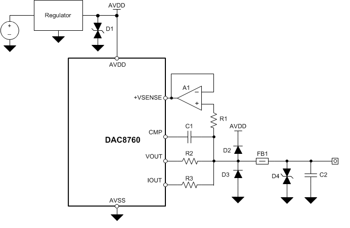
    You may refer to TIPD153 where the protection circuit is discussed in a bit more detail. The most ideal situation is to have series pass elements in between consecutive diode stages as each diode will conduct to a different potential and without this impedance the current flow between adjacent stages is only limited by trace impedance, which is typically quite low. When large currents flow through TVS diodes the reverse-breakdown voltage increases closer to the clamp-voltage, through clamp/steering/Schottky diodes the forward voltage increases closer to the maximum forward voltage. The intention of this external circuit is both to reduce the voltage and current that the DAC pins would see in the event that they were exposed directly to EMC/EMI transients such as what is documented in the IEC61000-4 standard as ESD, EFT, CI, RI, and Surge test standards.

    When using combined terminals the scheme changes a bit. TIPD119 documents the analog compensation technique for the leakage path that IOUT sees with large resistive loads through the VSENSEP pin. I made a quick drawing below:

  • Duke-san,

     Thank you very much for your prompt reply and
     detailed explanations.

     Your answer is very helpful to me.

     Please let me ask you an additional question.

     According to TIPD153, I think that it would be better to connect
     the C1 capacitor between CMP pin and VOUT pin.
      *Please see the attached file.

    Circuit.xlsx

     Is my understanding wrong?

    Best regards.
    Tsuyoshi Tokumoto

  • Tokumoto-san,

    Your understanding and diagram are both correct.

    Thank you.

  • Duke-san,

       Thank you very much for your prompt reply!


    Thank you and best regards,
    Tsuyoshi Tokumoto