Other Parts Discussed in Thread: DAC38J84
Hi,
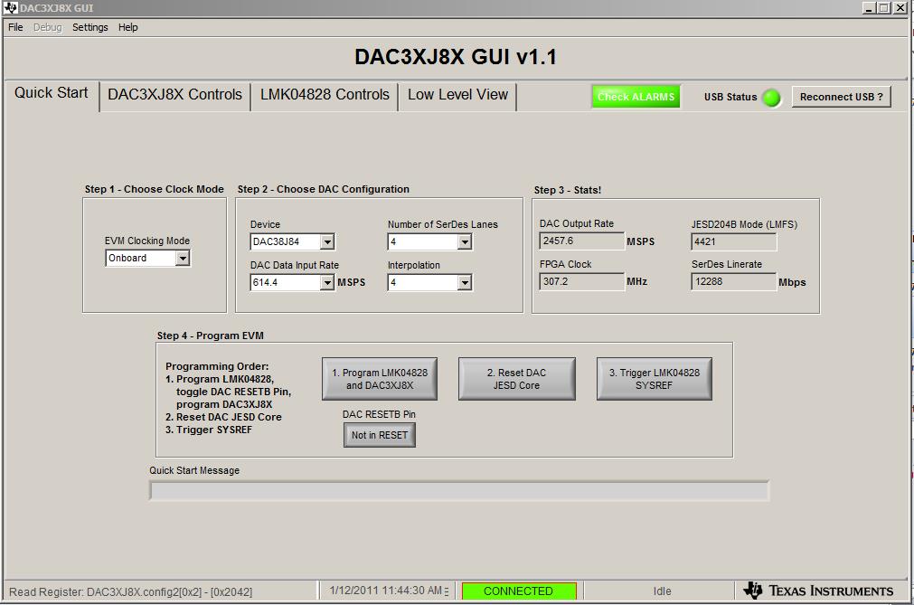
I am working with the DAC38J84 EVM and noticed that the FPGA clock is 1/2 the DAC Input Data rate and was wondering where those two numbers come from? In my application, I am running the device in 4421 mode with a sample clock = 2457.6Msps, this gives a lane rate of 12288Mbps. With by-4 interpolation, I understand that the input rate must be 614.4MSPS for the lane rate numerology to work out correctly, but I'm just wondering how the x2 is handled in the FPGA. Prsumably the FPGA fabric is running at 307MHz and somehow the data rate is doubled before it is serialized?
Thanks!
Below is a screenshot of my setup: