This thread has been locked.

If you have a related question, please click the "Ask a related question" button in the top right corner. The newly created question will be automatically linked to this question.

ADS42LB69: ADS42LB69 data output issue

Expert 1780 points

Part Number: ADS42LB69

Hello,

    We started testing the ADC output to FPGA Interface and observed the following:
1) The ADC was configured to send out all 1s and 0s and the FPGA read them correctly. 
2) Then we tried the alternating pattern (register value 0x33) but we get alternate 0xFFFF and 0x0000 (some realignment of data is occurring)
3) We tried the deskew pattern (0xAAAA), instead 0x5555 is being received
4) 8-point sine wave: periodic values with period 8 are being received but all are incorrect. 
The problem is that we are not getting the correct data, so there is some data alignment issue. 

There is no problem of noise/timing in our opinion because the numbers do not change with time (we acquire data in snapshots of 1024 words at a time) and have done many runs

We are interfacing this to a Xilinx 7 FPGA and the signal flow inside the FPGA is as follows:
1) data goes to IBUFDS and then IDDR (we tried different configurations for the IDDR (opposite_edge, same_edge and same_edge_pipelined), the results are similar (all of them give incorrect values)
2) clock goes to IBUFDS and then IBUFG (the adc_bit_clk_bufds_bufg is used as the clock source for the IDDR)
The data bit clock has been put under timing constraints. 

The register configuration for the ADC is:

Hard reset the IC and then,

1) Writing 0x01 to 0x15 (enabling DDR mode) 

2) 0x03 to 0x0F (setting the ADC to send test pattern data)

Are we missing anything in the register settings? 

Thank you for your time in helping us out,

Regards,
SM

  • SM,

    Are you setting the ADC output data format correct (2's comp vs offset binary)? Have you tried adjusting the DDR timing using register add 0x16? Is the routing of the CLKOUTP/N reversed going into the FPGA? What does the ramp test pattern look like?

    Regards,

    Jim

  • Hello Jim,

                Thank you for the inputs. 

    Would the output data format matter (2's comp or offset binary) for test patterns?

    We re-checked CLKOUTP/N, it is not a problem.

    1) For toggle pattern from the ADC:

    Getting alternate 0xFFFF and 0x0000 (incorrect)

    2) De-skew pattern is correct (getting 0xAAAA)

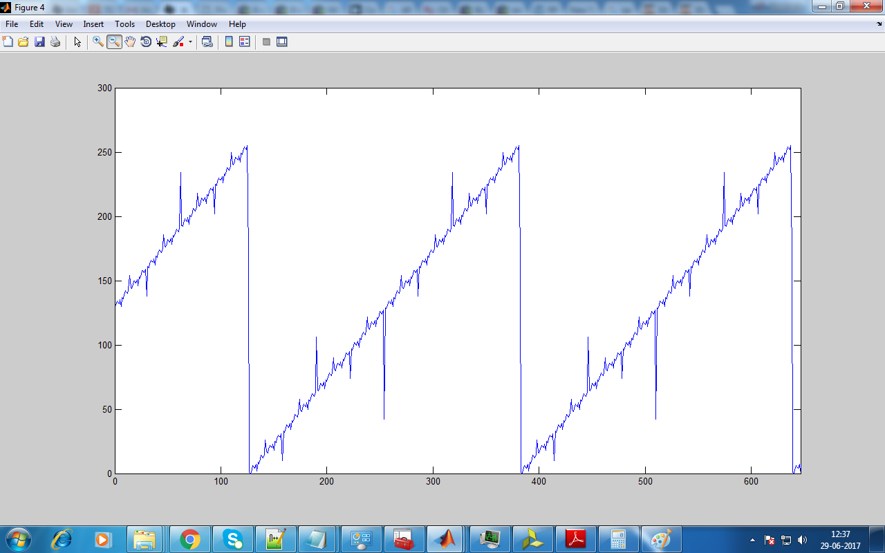
     3) For ramp pattern from the ADC:

    We are presently using the IDDR in same_edge_pipelined mode. When we looked at the individual bits, and found that the output of the IDDR had to be swapped (not sure why though). 

    So now we have something more like a ramp, but it is noisy. 

  • SM,

    After power up and a reset, program the ramp and DDR output format,  you should see the following:

    add 0x06   data 0x80

    add 0x08   data 0x18

    add 0x0D  data 0x6C

    add 0x0F  data 0x44

    add 0x15  data 0x01

    add 0x1F  data 0xFF

    I did see a capture similar to yours with one of our bad TSW1400EVM's. I believe your issues are with the timing inside your Xilinx device. Running slower should prove this to you.

    Regards,

    Jim

  • Hello Jim,

               The problem is almost solved now. I had to change the edge settings of the IDDR and the ramp looks fine now. 

    A small issue with the sine wave output: 

    As per the datasheet for register 0x0F: 

    1011 : 8-point sine wave: In the ADS42LB69, data are a repetitive
    sequence of the following eight numbers, forming a sine-wave in twos
    complement format: 1, 9598, 32768, 55938, 65535, 55938, 32768, and
    9598.

    I am getting a sinewave but with the following values: 

    0
    23170
    32767
    23170
    0
    42366    ---- these three correspond to the negative values in signed twos complement notation
    32769
    42366
    0

    The other test all give out the correct values: i.e., all ones, all zeros, ramp, toggling pattern, deskew except this one. Please advise,

    Regards,

    SM

  • SM,

    I am getting the same values as you. This may be a typo in the data sheet. I will check with the designer.

    Regards,

    Jim

  • SM,

    We just processed your observation. It matches with what the datasheet gives. We believe your are capturing data as straight binary. To convert a straight-binary format into 2's complement format, you just need to flip the MSB. This is equivalent to subtracting 32768 when data was smaller than 32768, and adding 32768 to what data was greater than 32768. See attached calculator spreadsheet.

    Regards,

    Jim

    Copy of 8-Point_Sinewave.xlsx

  • Thanks Jim.