This thread has been locked.

If you have a related question, please click the "Ask a related question" button in the top right corner. The newly created question will be automatically linked to this question.

ADS1262: Strange currents on AD inputs

Part Number: ADS1262
Other Parts Discussed in Thread: LM5165

The AD normally reads correctly. Rarely (1% of the times) after it is initialized it starts reading some 5% less; the input is differential with a voltage divider:

AVDD --|10K|-- AIN0 --|10K|-- AIN1 --|10K|-- AVSS

When this happen the behavior persists till the ADS1262 is reset and reinitialized.

We are using an AD1262 with:

No conversion Delay, FIR, NO BIAS, PGA=BYPASS, Rate=10, IDAC1/2 OFF, VDAC disable,
Reference+=AVDD Reference-=AVSS.

Periodically we switch Signal+=AIN0, Signal-=AIN1 and Signal+=AIN2, Signal-=AIN3; the behavior is the same on both channels.

If instead we switch on ANALOG POWER SUPPLY MONITOR  the drop in reading, when it happens, is about 30%

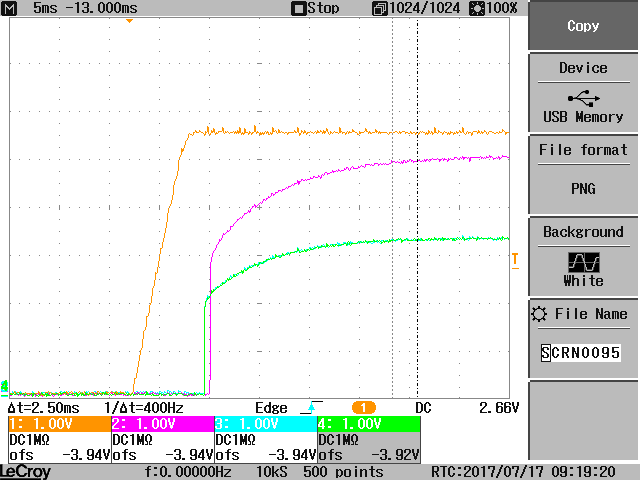
On the oscilloscope we noticed that  AIN0 drops 50mV and AIN1 rises the same amount when they are switched into the MUX; so it seems that the AD is sourcing/sinking some current.

Same for AIN2 and AIN3.

We patched the problem by checking the POWER SUPPLY MONITOR after reset using ANALOG SUPPLY as reference: if the reading is off by more than 10% of 1/4 FSR we reinitialize.

  1. This seems to work, but we would be interested in understanding the origin of the problem.
  2. What is the tolerance in the POWER SUPPLY MONITOR? Just to know if our patch is safe.

  • Hi Carlo,

    Welcome to the TI E2E forms!

    The problem sounds like it could be related to input bias current and/or loading on the AVDD and AVSS supplies.

    Have you tried probing AVDD and AVSS while switching the input MUX to see if the supply voltages are stable? Measuring the internal (AVDD-AVSS)/4 supply monitor will put a small load on the supplies, exactly how much I'm not sure, but it sounds like you are seeing more voltage droop when measuring the supply voltages.

    Additionally, I might recommend trying the above test again with the PGA enabled. Enabling the PGA will increase the ADC's input impedance and should help reduce the effects of input bias current on the voltage measurement.

    Between the above two suggestions, I think you'd be able to get a better feel of whether the issue is related to supply loading or input bias current.

    Regarding your second question, I'll need to look to see if we have any information on the supply monitor tolerance...

    Best regards,
    Chris
  • Dear Chris,

    my patch of resetting the AD if the reference is out of more than 10% reduces the event frequency from ~1/100 to ~1/20000; sometimes, even resetting the pin repeatedly (up to 10 times) would not work.
    Inserting the PGA x1, as you suggested, resolved the problem: I was able to stop a unit while exhibiting the problem an tried inserting and removing the PGA repeatedly: with PGA it was ok, without the problem reappeared.
    Still I think something is wrong: it looks like that, when power is cycled, sometimes the AD wakes up in a way that the input impedance of the internal ADC module is significant lower; sometimes this may be cured by an hardware or software reset, sometimes it cannot.
    With the 10K resistors bridge the impedance each input line sees should be <=10K (the other path is occupied by the current of the other input); if the input current is <150nA, the variation of the voltage on the input should be less than 1.5mV, not the 50mV i see on the scope as above.

    Best regards,

    Carlo
  • Hi Carlo,

    Would you be able to share a schematic of your circuit? That would be helpful to me. (Feel free to send it to pa_delsig_apps@ti.com instead of posting it to the forums.)

    I'm still not sure if the issue is input bias current related or not, since there seems to be a lot of dependencies to the AVDD and AVSS supplies...

    Is the problem only occurring when you use the analog supply monitor, or is it just getting worse when you use it?
    FYI: The supply monitor adds a 200kOhm load between AVDD and AVSS.

    Do you see the effects of the 50 mV voltage drop in the conversion results?
    Since you're using the AVDD and AVSS supplies for the ADC's reference, I would expect that the ADC output codes would not change significantly if AIN0/AIN1 are changing proportionally to AVDD/AVSS.

    What are you using to supply AVDD and AVSS? How much current are these sources able to supply? Is it possible that you might be running into a current limit? Did you try probing AVDD and AVSS to see if they were stable?

    Are there input signals being applied to the ADS1262 before you power up the analog supplies or are the inputs coming up as the supply ramps? If, during power up, your inputs are at a higher potential than the analog supplies then you might be turning on the internal ESD diodes and getting a higher than normal input current.

    Thanks and best regards,
    Chris
  • Dear Chris,
    I am sending you a schematic by email.

    I started testing, as I told you, with a 5VOUT-10K-AIN0-10K-AIN1-10K-AGND bridge.
    From what you say, I guess that when I measure the analog supply I have a similar configuration with 50K, 100K and 50K, so that the effect of the currents is proportionally higher.
    As you see on the scope image the problem is there using the external 10k-10k-10k bridge and it is reflected in the measures that change some 5%.
    When using the internal 200k bridge the error increases to 30% (6 times the resistance, 6 times the error).
    The error is only visible when the PGA is bypassed, so it seems that the currents originate on the right of the PGA (in the schematic on the data sheet).
    When the problem occurs at power up, I can keep inserting the PGA x1 or bypassing it and the problem accordingly disappears and reappears. Resetting the ADS1262 most of the times solves the problem, but occasionally a power cycle is needed.
    AVDD is stable at 5V; the circuit in normal operation drains 5mA at 24V, so the whole current at 5.5V (on the output of the LM5165) is around 20mA. This is then split between the 5V and the 3.3V rails.
    The inputs of the ADS1262 are set by a FET controlled by AIN8, so that there is no possibility that the voltage is there before the ADS1262 is initialized.
    The problem was first noticed when the inputs of the AD were connected to the analog outputs of a MURATA SCA103 inclinometer; this device has a ratiometric output, so it is not influenced by supply changes and the error was some 0.5% of FSR.
    The only information I could find related to the SCA103 output impedance is "Analog resistive output load minimum 10KOhm"

    Best regards,
    Carlo
  • Hi Carlo,

    I'm sorry I had the incorrect email address above. If you would, please resend the email to pa_deltasigma_apps@ti.com and I'll take a look at it.

    Thank you,
    Chris

  • Hi Carlo,

    Thanks for the schematic, I got this time!

    Is this problem occurring before you configure the ADS1262?
    By default the PGA should be enabled after power-up, so it is only after disabling the PGA that you see the additional input bias current?


    I think you might have a power-up issue...

    The LM5165 in PFM mode can only source a maximum 100 mA, so this is the maximum current available to the 3.3V and 5V power rails combined.  During power-up, I'm certain that the in-rush current will exceed 100 mA. The ADS1262 can sink more than 100mA during power-up; and all of the supply bypass capacitors will behave like short circuits, sinking large currents as they charge up. This could be causing some very odd behavior and might explain the occasional need to power cycle your circuit.

    You might try...

    • (if you can) ...to perform a controlled start-up:
      • Ideally, you would want the 3.3V and 5V LDOs to be disabled until the LM5165's output was settled and then to have them enable one at a time. This could be done by connecting the PGOOD signal to the 3.3V LDO's SHDN pin (see figure 36 in the LM5165 datasheet; NOTE: that a pull-up resistor is required for this signal), and then by using a GPIO signal from the micro to the SHDN pin on the 5V LDO to enable the 5V supply sometime after the 3.3V supply was settled. While powering up the 5V rail, I would recommend keeping the /PWDN pin of the ADS1262 low until the 5V supply had settled (NOTE: a pull-down resistor on /PWDN would ensure that this signal is low while the micro powered up).
    • ...connecting external 3.3V and 5V sources with higher current outputs to provide additional start-up current.
      • You have the 3.3V supply pinned out, so you might just try running that supply from an external bench source and holding the ADS1262's /PWDN pin low with the micro until after the 5V supply has settled.

    Best regards,
    Chris

  • I checked the startup of the supply; it looks fine to me.

    The green line is the power good from the LM5165; it is pulled up to the 3.3V rail, because it is also connected to the CPU, but it is obviously released from the internal open collector when the 3.3V line ramps up.

    The 5.5V line (yellow) out from the LM5165 seems perfectly stable while the green 3.3 V and violet 5V supply ramp up.

    Quite rarely the spurious current effect has been observed even when the PGA is activated (something like 1 in 10000 times) when switching power.

    So, resetting the AD multiple times if measuring AVDD via internal resistor bridge fails helps

    Using PGA x1 helps.

    But neither completely solves the problem

  • Hi Carlo,

    Did you mean to attach an image?...if so, it didn't seem to come through.
    (For some reason, copying and pasting images into the Forum text box doesn't work too well. You may need to use the rich text editor and use the "Insert Media" button, shown below...)


    Do you currently hold the /PWDN signal of the ADS1262 low during start-up, while the supplies settle? I would suggest trying a longer delay before starting-up the ADS1262, as it would seem that the ADC is not powering up correctly if  resetting the device resolves the issue.

    Also, do you know if the issue is occurring with the ADC's default settings (PGA enabled), or is it only AFTER bypassing the PGA that the problem first appears?

    Thanks and best regards,
    Chris

  • Here is the startup of the power supplies:

    The Powerdown line is low for about a second after startup before initialization starts.

  • Now instead of resetting the chip (short low pulse on RESET/POWERDOWN) I force a powerdown with a long low pulse.
    If this fails I retry with longer low pulses (40, 40, 40, 200, 400 mS).
    In a test with 3000 cycles each on 12 units the problem has not occurred again.
    We will proceed with more testing; I will let you know if this really solved the problem.
  • Hi Carlo,

    Sorry for the delay. I'm glad to hear that you've made some some progress on this issue though.

    Looking at your last oscilloscope screenshot, the power rails do appear to come up cleanly. However, have you tried probing the power rails when setting the ADS1262's /PWDN pin high, to see if there are any glitches around the time that the ADC is enabled? I might also suggest probing the input pins at about the same time (and around the time you bypass the PGA) to see if you can see any glitching there as well.

    Another suggestion I might make to your existing circuit would be to control the 5-V LDO's enable pin and enable it with the microcontroller AFTER the 3.3-V supply has settled. My rationale for doing this would be to allow the ADS1262's digital circuitry to settle before enabling the analog functions which are controlled by the digital logic. This might prevent odd behavior due to the GPIOs, IDACs, and other analog functional blocks not powering up into a well-defined state if DVDD is still ramping.

    ...Better yet try monitoring the ADS1262's internal 2-V digital supply on the BYPASS pin to get an idea of how long it takes for the internal digital supply to settle (I believe this should be less than 50 us after the 3.3V supply is settled), and make sure you enable AVDD only after the internal 2-V supply is settled.

    I can't think of a much smoother power up sequence then to delay the 5-V LDO enable signal, and then bring the ADS1262's /PWDN pin high some time after that.

    Also, make sure that after setting the /PDWN pin high that you wait about 10-50 us for the crystal oscillator to settle before trying to communicate with the device. A best practice would be to wait for a /DRDY signal before sending any SPI commands, as you can know for sure that the crystal is oscillating and the device is ready for SPI communication by that point.

    Best regards,
    Chris