Hello!
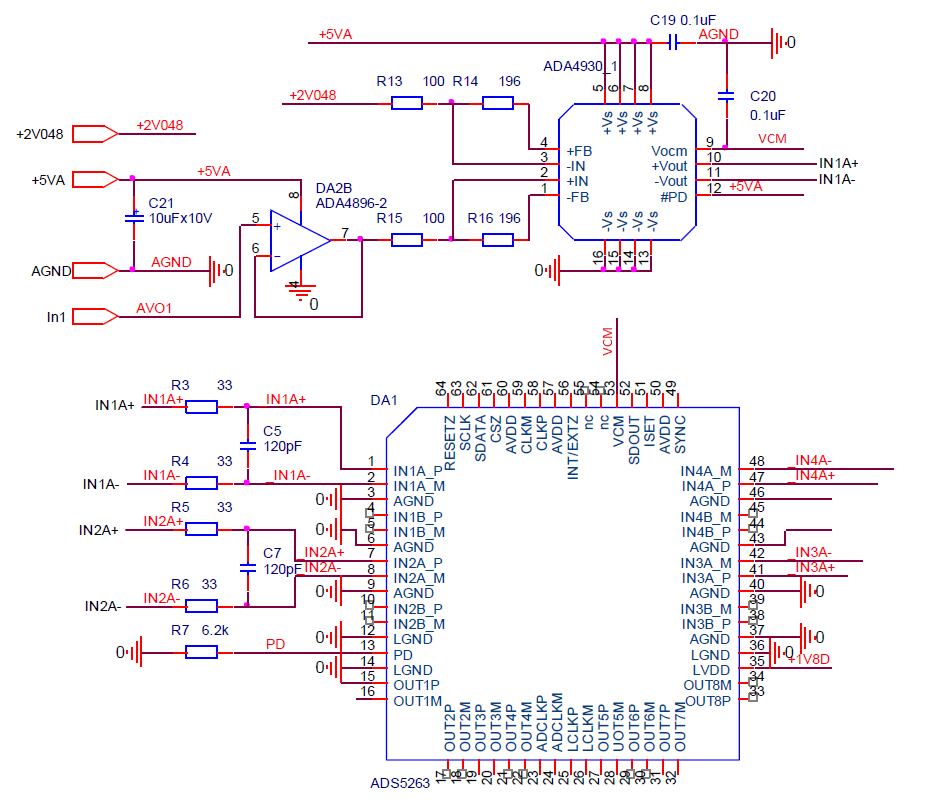
We are using ADA4930 to drive ADS5263. Maximum slew rate of the signal at the input of ADC is 47V/us. Acquisition Time should be ~85ns. Here is a fragment of the circuit:

Are there any mistakes in our design? I'm confused by the phrase in ADS5263's datasheet (page 63): "A 5-Ω to 15-Ω resistor in series with each input pin is recommended to damp out ringing caused by package parasitics. It is also necessary to present low impedance(<50Ω) for the common mode switching currents. This can be achieved by using two resistors from each input terminated to the common mode voltage (VCM)."
1) Why do we what to place those 5-Ω to 15-Ω resistors in series with each input? I think we need a little a possible impedance between "reservoir" capacitor C5/C7 and sampling circuit of ADC.
2) Could you explain why I need "two resistors from each input terminated to the common mode voltage"?
Another question is about analog input equivalent circuit (figure 90 page 62). I'd like to simulate glitches caused by sampling circuit.

3) What are timing diagrams of those three switches? Sampling switches are "off" during convertion period and they are "on" rest of the time. Right? What is timing diagram of the third switch (rightmost)?
Thank you!