A related question is a question created from another question. When the related question is created, it will be automatically linked to the original question.
If you have a related question, please click the "Ask a related question" button in the top right corner. The newly created question will be automatically linked to this question.
You are correct. If LED D8 becomes illuminated, it means that there is a DRAM issue. (Just to be clear, you are able to connect to HSDC Pro, but error happens when you try to capture?)
Unfortunately, the board must be replaced. Please return it to TI through your appropriate channels. Before you return the board, could you please provide the serial number that is associated with the board when connecting to HSDC Pro? Thank you!
All applogies, but please do not return the board yet. I need to revisit this issue, as it appears I was incorrect in my initial diagnosis. I will replicate your setup in the lab, and see if I get similar results.
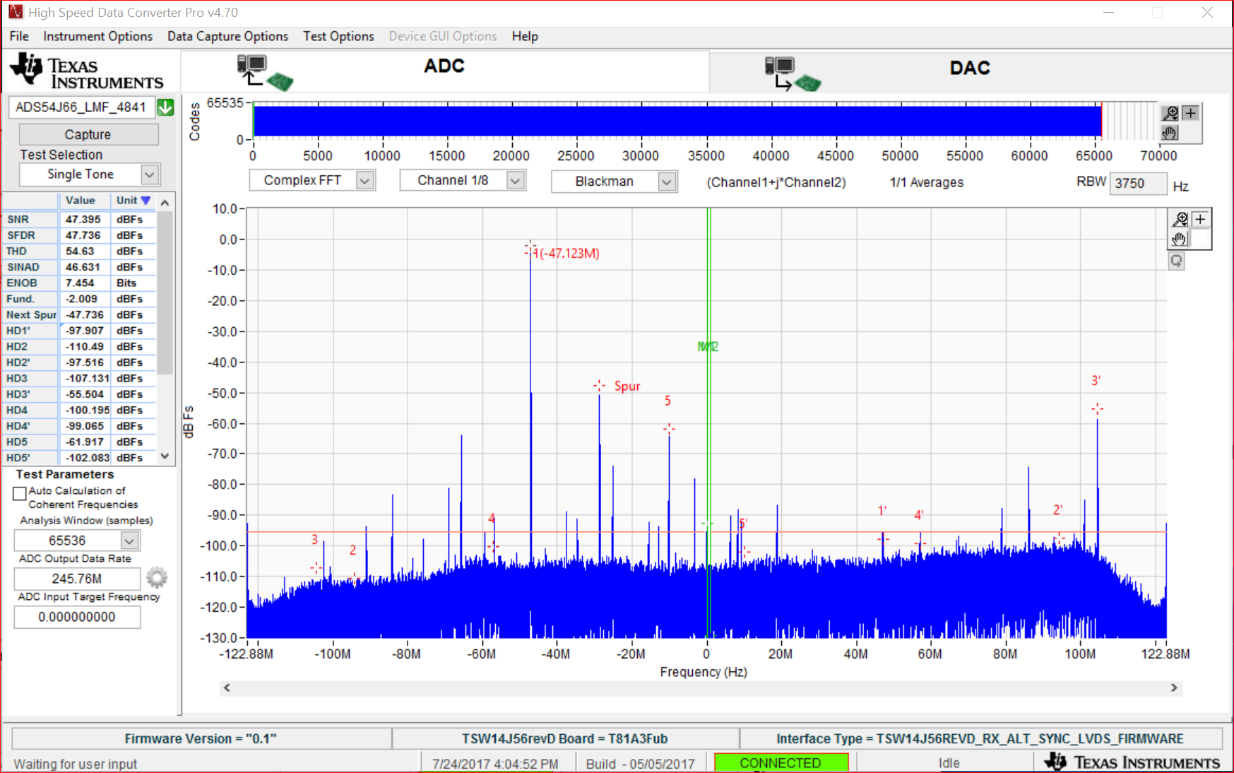
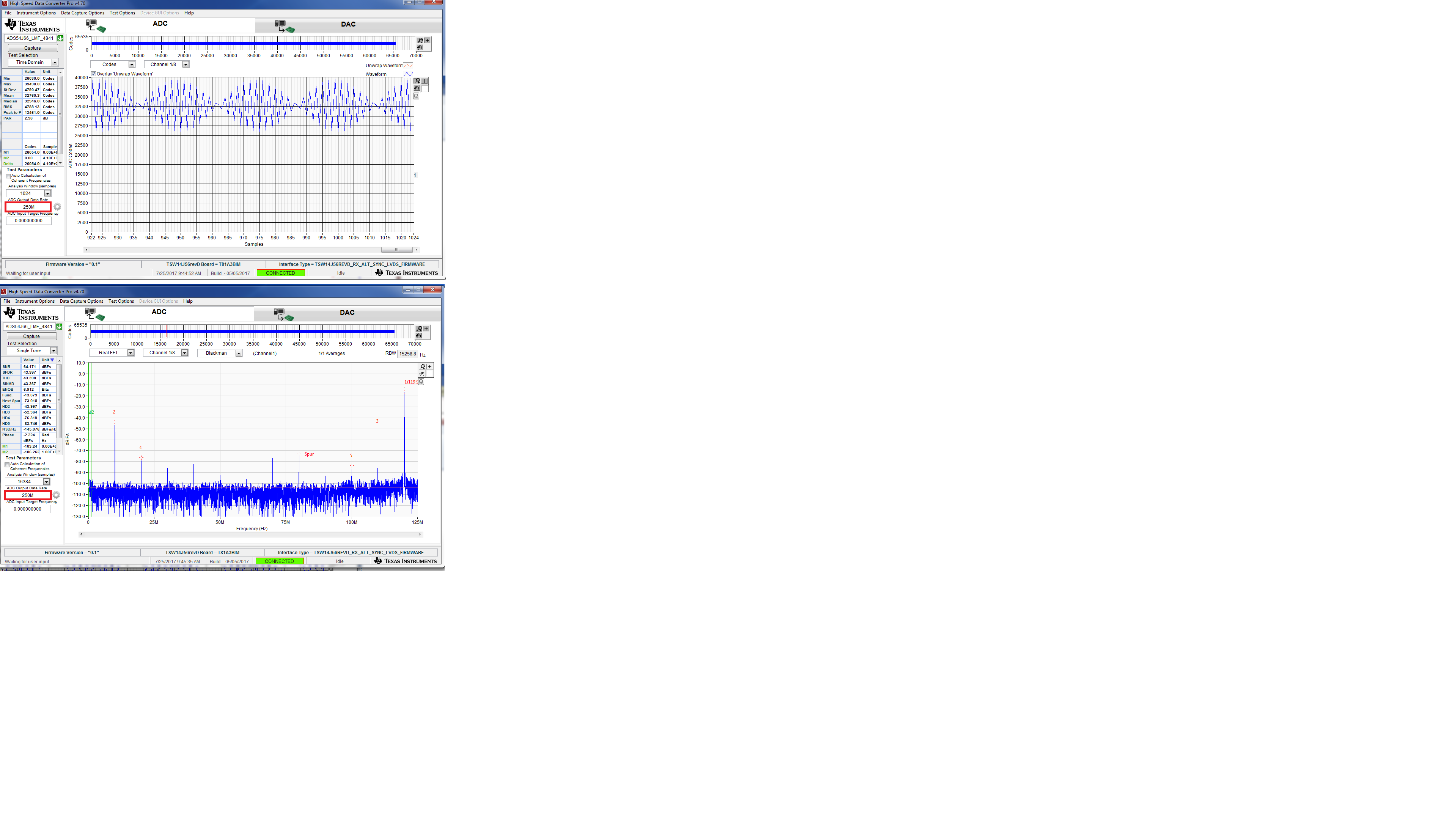
I was able to get the ADS54J66 to capture by using the quick start section of the user's guide. Please ensure that you follow these steps, as written, in order to prove that the hardware is functional. Also, please ensure that the ADS54J66 power supply can supply more than 1A (mine draws around 1.3 amps after configuration files are loaded).
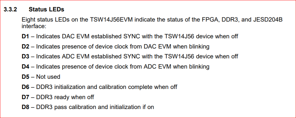
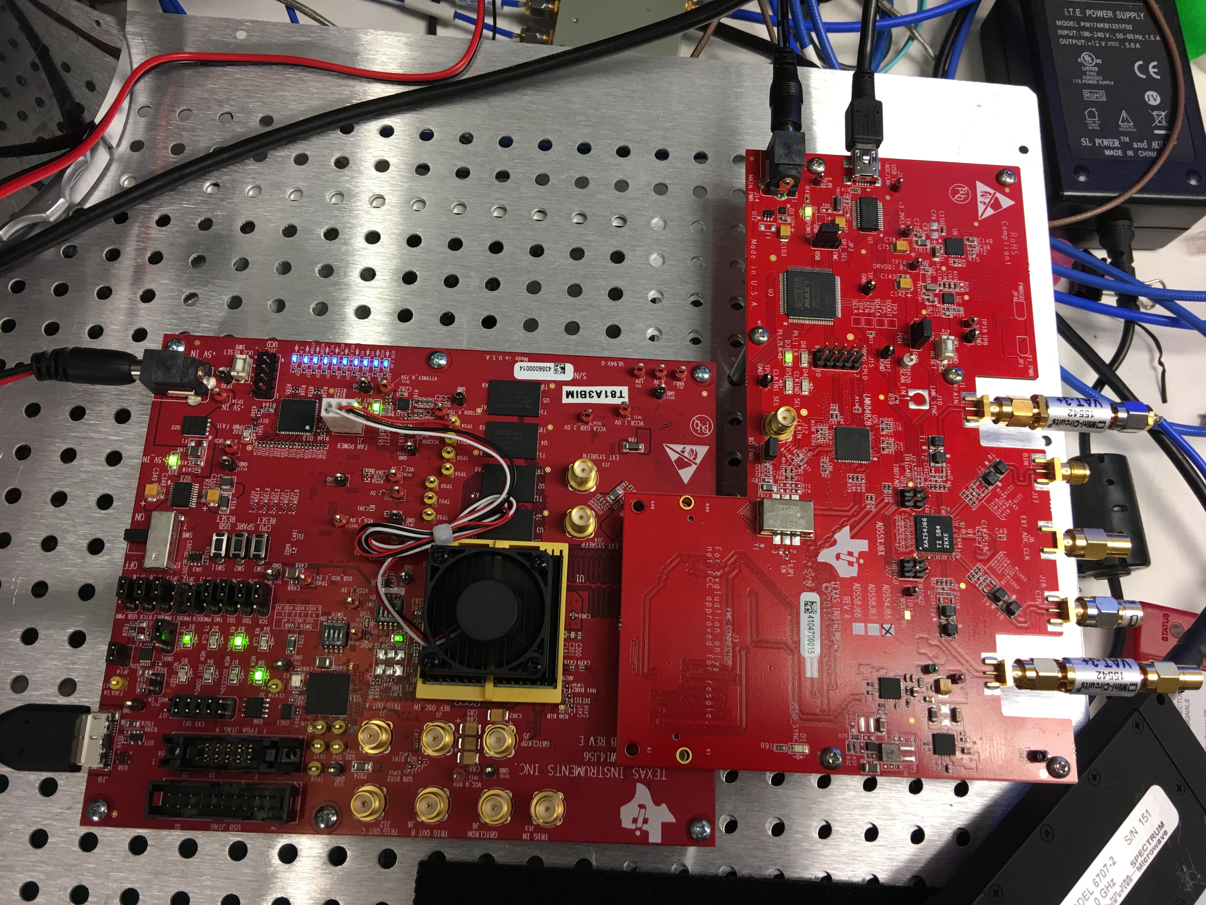
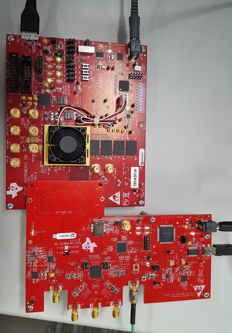
After making all connections and loading HSDC Pro firmware and ADS54J66 configuration files (as shown in quick start guide), your setup should look like the picture below.
After entering ADC Data Rate and clicking "Capture", your setup should look like this. Notice that D3 on ADS54J66 illuminates after loading the first configuration file in the ADS54J66 GUI.
Notice that D3 has extinguished and D4 is now flashing. HSDC Pro should have a capture that looks something like this.
Could you please tell me (or screenshot) what error HSDC Pro is giving you?
From your photo, it looks like you have an early version of the ADS54J66EVM because the ADC device is labeled as a pre-production unit. Send us your address and we will get you an updated EVM ASAP.
The last October we bought several ADC/DAC boards for evaluation, but we received this March.
The ADS54J66EVM is one of eval board and I am trying to test with TSW14J56 board.
You think ADC model issue? Not an FPGA/DDR problem right (I can hold return process)?
We have the plan to development prototype 499.680 MHz RF bunch digitizer for our machine diagnostics ( NSLS-II facility ).
RF input is 499.680 MHz, Fs sampling frequency also 499.680 MHz.
If you send me updated board that's appreciated for our evaluation.
I also ordered an ADS54J60EVM eval board (1 Gbps 2 channel ) for performance evaluation.
Shipping address :
Kiman Ha
Accelerator controls group
Bldg 741
P.O.Box 5000
Brookhaven National Lab
Upton, NY 11973
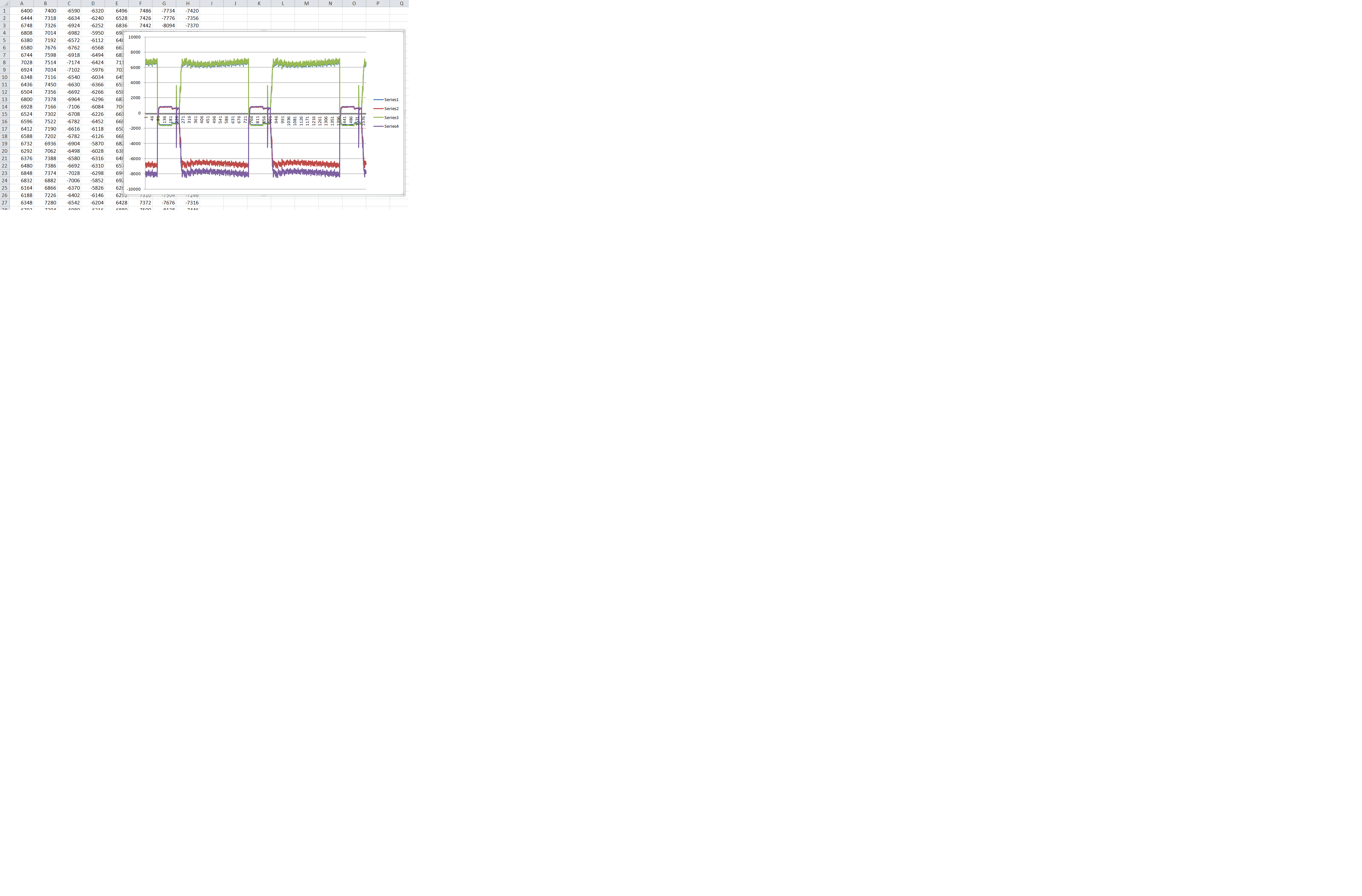
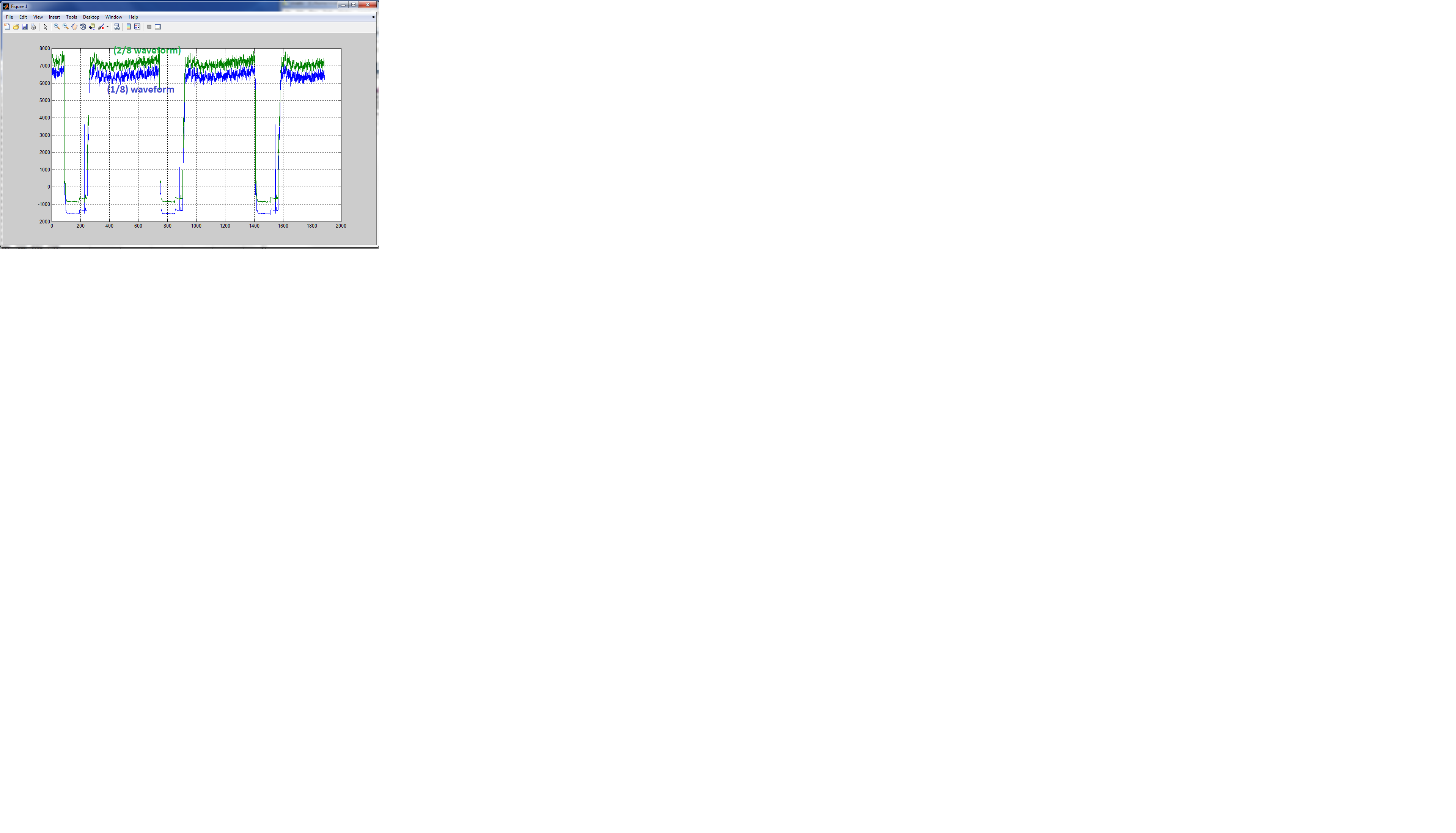
To make the routing of the analog traces symmetrical and keep everything on the top side of the board, we swapped the P and N signals of channels 1 and 3 going to the ADC. This is why you are seeing what you are.