This thread has been locked.

If you have a related question, please click the "Ask a related question" button in the top right corner. The newly created question will be automatically linked to this question.

ADS8568: Suitable microcontroller

Part Number: ADS8568
Other Parts Discussed in Thread: DAC8563, ADS8584S

Hello,

I'd like to use an ADC which has 16-24 bit precision, high sampling and 4-channel bipolar input of +-2.5V . ADS8568 seems interesting to me however it has 8 channels. Do you have 4-channel version which has a similar (and simple) architecture like ADS8568?

Can you recommend a microcontroller  which is suitable with DAC8563 and ADS8568 together in order to use in a battery powered, precise and fast, portable biomedical device? It should have minimum 3 SPI + 1 SD card interface. 

Thanks in advance,

Handenur

  • Hello Handenur,

    Thanks for your query on E2E forum. Unfortunately we don't have 4-ch version of ADS8568, but we a 4-ch similar architecture ADC, ADS8584S, which is 4-ch simultaneous-sampling SAR ADC with bipolar inputs on a single power supply, and it can operate at a maximum of 330 kSPS per channel, please check the datasheet at www.ti.com/.../description.

    Can you please let me know what sampling rate you want? do you need simultaneous-sampling or non-simultaneous-sampling ADC? What else requirements? 

    For microcontroller, it depends on what kind of resource/task you want, I'm not an expert, but I think MSP432 or MSP430 ultra low power MCU is good for you because your system is powered by a battery. You can go to MSP Low-Power Microcontroller Forum to get a professional advice:  e2e.ti.com/.../

    Thanks& Best regards

    Dale

  • Hello Dale,

    Since 8568 has simpler design I would probably choose it. As sampling rate 100kSPS or higher is possible, simultaneous sampling is a big advantage for me since I want to get the conversion results with the least delay possible.

    Thank you,
    Handenur
  • Hello Handenur,

    Thanks for your information, please let me know if you have any other questions about ADS8568.

    Best regards

    Dale

  • Hello Dale,

    I have a question regarding ADS8568 timing. There is CONVST_x signal and I didn't understand its main function.  

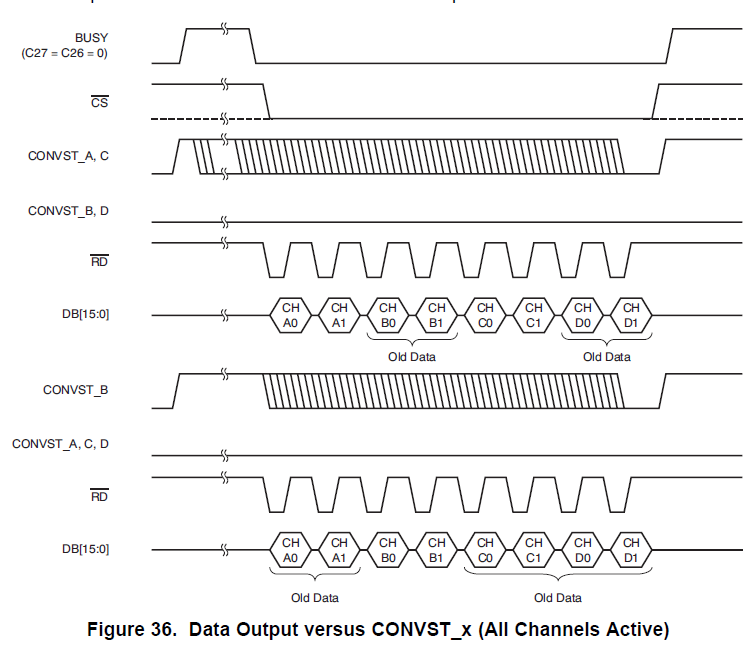
    Especially the diagram from datasheet below is not clear for me. Why do we need that convst signal? What is the reason behind showing the convst signal with so many cycles?

    Thanks,

    Handenur

  • I have one more question. I will use only four of the eight channels. Is it possible to get the data from only two channels (i.e. SDOA and SDOB) and connect the other two channels to ground (since I don't want to get any data from the other two channels) ?

    Can I also connect these two channels (i.e. SDOA and SDOB) with a two different SPI modules of an STM32 microcontroller's peripheral? In short I want to get 4 channel data as simple and quick as possible and send it to a microcontroller via SPI interface.

    Best,
    Handenur
  • Hello Handenur,

    The ADC’s conversion will be initiated by the rising edge of CONVST_x signal which is controlled by CPU/FPGA, many ‘cycles’ after available CONVST_x signal means that it can be pulled down at any time, but it’s a good practice to pull CONVST_x low after detecting the conversion is completed and BUSY is low by checking BUSY’s falling edge.

    For your other questions, Parallel interface is faster to get the data than serial interface.

    Parallel interface:   

    • Software mode:     switch off unused channel pairs by setting the Configuration register bits C22, C20 and C18 (PD_x), then only send out related two CONVST_x signals, and four /RD pulse to read four channel data.
    • Hardware mode:    only send related two CONVST_x signals, and four /RD pulse to read first four channel data(CH A0/A1/B0/B1).

    Serial interface:   

    • Power down unused channel pairs by setting the Configuration register bits C22, C20 and C18(PD_x), only enable SDO_A and SDO_B outputs, send out related two CONVST_x signals.
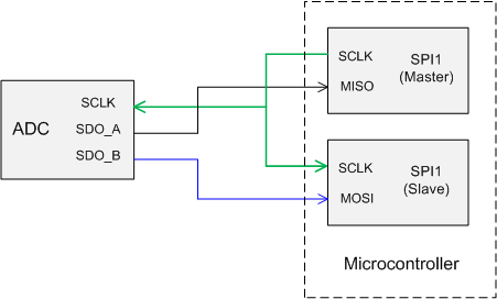
    • Two SPI modules can be used but one should be configured as master and another should be slave SPI because one same SCLK should be used for both SPIs, the SCLK from master should be clock input of slave SPI.
    • Maximum throughput rate is 400ksps by using two output ports.
    • Unused output ports can be left floating because they are output pins.

    Remark:    If only four channels are used, unused channel input pins(CH_C0/C1 and CH_D0/1)  can be connected to ground.

    Please let me know if you have more questions.

    Thanks&Regards

    Dale

  • Hello Dale,

    Thank you for the clarification. However, I didn't get what you mean by SPI master&slave config exactly. Your suggestion resembles daisy chain configuration however it is not the same?

    What I want to do is to connect SCLK and SS lines of SPI1 and SPI2 peripherals of the µC to the corresponding SCLK and FS pins of ADS8568; but just connect SPI1's MISO line to SDO_A and SPI2's MISO line to SDO_B. But I don't think that it is doable.


    Thanks,
    Handenur
  • Hello Handenur,

    It's not a daisy-chain mode. If both your SPI1 and SPI2 are used and configured as master mode, when you connect both SCLK of SPI1 and SPI2 to ADS8568's SCLK pin, ADS8568 will have two clock input sources on the same signal line, this is not acceptable because probably there is a difference between two clocks, the SPIs on CPU always latch and get the data on SDO with a SCLK signal, so the solution to use two SDOs on SPIs is to config one SPI as master mode and another SPI as slave mode, the SCLK of master mode SPI can be connected and used for the SCLK of slave SPI, both SPI interfaces and ADS8568 ADC will use the same SCLK source, then two SDO pins from SPI1 and SPI2 can be connected to SDO_A and SDO_B on ADS8568.

    Thanks&Regards

    Dale

  • Hi Dale,

    Could you explain this configuration with a diagram? I am sorry I still didn't get the point. Can I connect SPI1's (master) SCLK to SPI2's (slave) SCLK even though they are both on the microcontroller?

    Thanks,
    Handenur
  • Hello Handenur,

    Yes, that's what I suggested as well, please refer to a simplified block diagram as below.

    Thanks&Regards

    Dale