Other Parts Discussed in Thread: TINA-TI
Dear Community,
after several days of debugging and browsing quite a while through this forum, I was not able to find a solution or answer to this problem (see TITLE), even though the question has been there already.
I am using the ADS1299 in a hybrid acquisition setup, whereas 6 channels are used for EEG- Acquisition. The ADS1299 circuit was based heavily on the datasheet, application note and evaluation kit schematics - and the developed solution has been in use here for more than a year. The following details might be of interest:
- quasi-symmetric power supply from a battery (within the allowed range given in the datasheet): AVDD = +2.7V, AVSS = -2.55V, AGND = 0V
- pcb design as mixed circuit with split analog/digital grounds as recommended, star ground at analog voltage supplies
- DRL / BIAS feedback resistor/capacitors values are chosen as in the ADS1299 evaluation kit schematics: 1Meg Ohm / 1.5nF
- EEG AREF and BIAS buffer both use internal reference (AVDD+AVSS)/2 = -75mV (referenced to AGND)
- single-ended measurement of ch1-6 by using a common electrode to In1-6N (not SRB1, since channels 7-8 are used for another puprose)
- more in the following excerpt of the schematic
Register Configurations:
- When bias enabled but not measured: CONF3= b1110 1100
- When bias measured: CONF3= b1111 1100 and ChnSET bits[2:0]= b010
Now the Problem:
Depending on the configuration of the bias (turned on/off, using different combinations of inputs - BIAS_SENSP/ BIAS_SENSN), the bias signal often shows a significant DC offset, that is inexplicable to me.
When i measure the DC bias signal without with the SENS/N registers 0 (no inverting channel inputs to the bias signal), i measure a negligible dc offset, as expected.
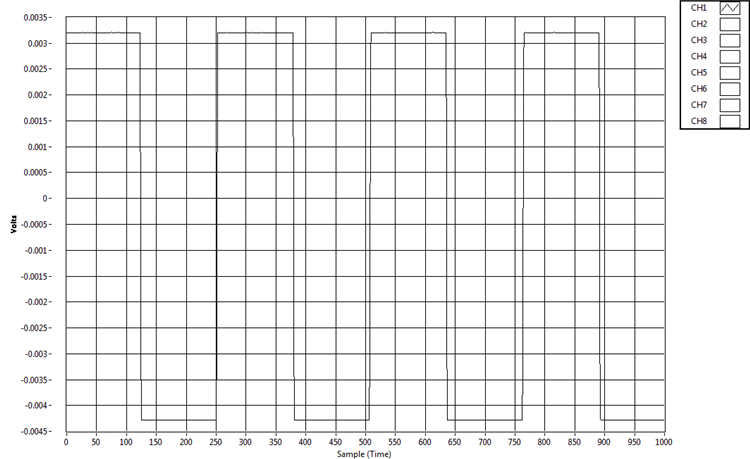
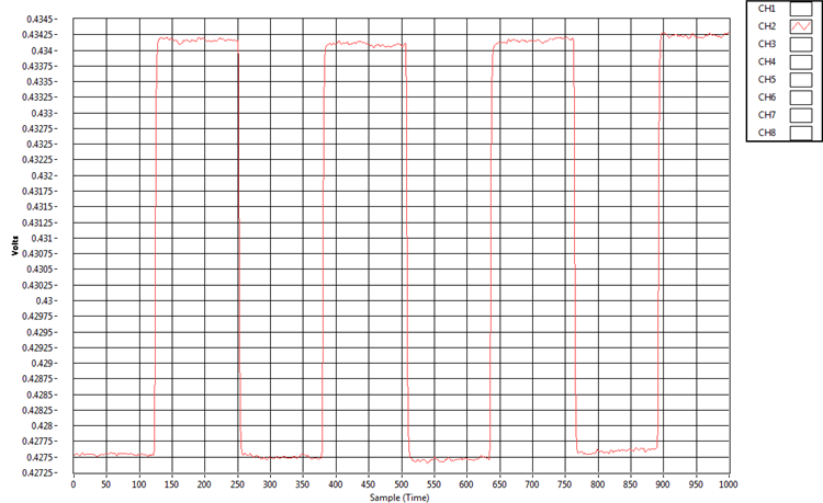
However, when any SENS registers are configured, i get dc offsets in the range up to the Volt-level, which results in clipping of the eeg-channels when Gains>1, in on-body measurements. Trying to investigate this and to give an example, I just the internal ADS1299 test-signal on CH1, set BIAS_SENSP to b0000 0001 and BIAS_SENSN all to 0, and measured the bias signal on CH2. Please see the following screenshots
As expected, the bias signal shows the inverted test-signal (which has a slight negative offset, see ch1) - however with a gain of G=-2.4 and adds an OFFSET of ~1.6V!!
The Gain is roughly the one expected from the TI 10 Applications and Implementation Note on the ADS1299 (Rev. C). here i expect (with Rf=1Meg) and N=1 (Number of Channels used for Bias Drive, here IN1P) a gain of G=3 or (if 220kOhm are used, these are actually the values shown in TI datasheets for the PGA resistors) of G=4.54.
A test for all input gain levels of CH1 (amplifying the test signal with G=1 up to 24) always resulted in a constant amplification of the ac signal (measured gain G=-2.4). The offset remained constant at around 1.6V when using only a single input channel to the Bias stage.
The small difference in gain from the expected one does not matter so much - the huge DC offset does however: With bias-signals with these dc-offsets on the body, the EEG-electrodes directly clip (for G>1) and I cannot measure a proper signal.
Of course I started evaluating with electrodes on the body - but ended up narrowing down the Problem to everything inside the ADS, to make sure it is not another physical problem of any kind in the external setup.
- adding channels to the bias can increase the offset up to to AVDD/AVSS
- The offset does not seem to result from the small dc offset in channel 1 and a huge gain of the DRL circuit. If it was so, the test signal would have to to be amplified with the same gain
- The dc-offsets do not always have the same levels. When used on the body, (with e.g. CH1 measuring EMG/EOG/EEG) and depending on the configuration of the SENS registers,the offsets can be also in the range of x*100mV.
Thank you very much on any notes and thoughts on this.
It seems there have been other people experiencing a similar problem in this forum but without a solution so far (see e.g. https://e2e.ti.com/support/data_converters/precision_data_converters/f/73/t/351795 .


