This thread has been locked.

If you have a related question, please click the "Ask a related question" button in the top right corner. The newly created question will be automatically linked to this question.

ADS1299-4: read continuous data from ADS1299-4

Part Number: ADS1299-4
Other Parts Discussed in Thread: ADS1299, ADS1299EEGFE-PDK,

Hello,

I am working on a custom board using ADS1299-4 , communication with the IC seems fine - ID number reads fine, control registers can be written and read, parameters such a continuous mode and sampling frequency seem to be set without problem. I am now at the stage to get data from ADS1299 but I am facing the issue of not being able to get valid data.

For example, for an uni-polar analog power supply of 5V, when using ADS1299EEGFE-PDK to read the mid-supply value through channel 1 I am getting ADC code of 0x00470F4D and voltage of 2,498142V which both seem correct. With my custom board, however, values I am getting are quite random and do not seem valid - while I am expecting to get ADC code of about 0x00470F4D what I am getting is a sequence of numbers quite random and different from each other, such as

h1 data: 007FFFF0; ch2 data: 00456920
ch1 data: FFFF444A; ch2 data: FFEF0000
ch1 data: FFB3439A; ch2 data: 00020000
ch1 data: FFA345F9; ch2 data: FFB50000
ch1 data: 00664454; ch2 data: FF890000
ch1 data: 007FFFAA; ch2 data: 0044EC74
ch1 data: FFA441F2; ch2 data: 00350000
ch1 data: FFE34533; ch2 data: FFE10000
ch1 data: FFA644AA; ch2 data: 00780000
ch1 data: 006444C1; ch2 data: 007D0000
ch1 data: FFB044C1; ch2 data: 007B0000
ch1 data: FFAD4638; ch2 data: FF970000
ch1 data: FFA64460; ch2 data: 00770000
ch1 data: FFE74545; ch2 data: FFCC0000
ch1 data: FFDC4519; ch2 data: 00060000
ch1 data: 000045B9; ch2 data: 00770000

With other kinds of measurements the situation seems similar, the mid-supply measurement seems to be the most suitable to test the measurement mode, however.

I will be grateful if someone give advice how to debug the problem...

  • Hello Kamen,

    Thanks for your question.

    Can you please share the register settings that you are using for the measurements on your board?

    To verify the device operation, you could try probing the reference voltage and the supply voltages to confirm they are configured as expected. I assume you are still using a unipolar 5-V supply and the internal 4.5-V reference? If you'd like, you can also share the ADS1299-4 section of your schematic and we can review the relevant connections.

    Best Regards,
  • Dear Ryan,

    Thanks for reply. Below I provide the required details. What I feel is that I am reading the data from the ADS1299 somehow in a wrong manner, however I can't yet figure out what I have overlooked.

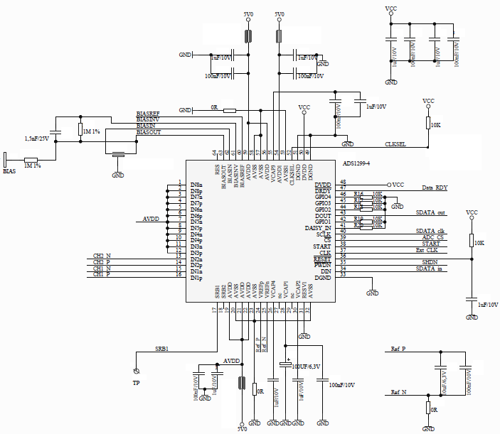
    Indeed, I am using a uni-polar power supply 5V (measured it - the 5V voltage is fine), internal reference (measured voltage BIAS_OUT-GND, and BIAS_INV-GND - it is as expected 2.5V). On the schematic below BIASREF, CH1 P, CH 1 N, CH2 P, CH2 N, SRB1 are floating - not yet connected - I believe these do not need to be connected to see the correct internal test signals. 

    The ADS1299-4 connection is as follows:

    ADS1299 configuration is as follows:

    /*******************************************************************************
    *
    * ADS1299 register configuring
    *
    ********************************************************************************/
    static BYTE ads1299_cfg(void)
    {
      BYTE settings;
    
      //===================== configure and activate channel #1
      settings = 0x00;
      settings &= ~CHANNEL_POWER_DOWN;      // enable power to the channel
      settings |= ADS1299_PGA_GAIN01;  
      settings &= ~SRB2;                    // we don't make use of SRB2 pin in our app, so it is open  
      settings |= ADS1299_INPUT_SUPPLY;                    
      ads1299_write_reg(CH1SET, settings);
    
      settings = 0x00;
      settings &= ~CHANNEL_POWER_DOWN;      // enable power to the channel
      settings |= ADS1299_PGA_GAIN01;
      settings &= ~SRB2;                    // we don't make use of SRB2 pin in our app, so it is open  
      settings |= ADS1299_INPUT_SUPPLY;                    
      ads1299_write_reg(CH2SET, settings); 
    
      settings = 0x00;
      settings |= CHANNEL_POWER_DOWN;       // disable power to the channel
      settings |= ADS1299_PGA_GAIN01;
      settings &= ~SRB2;                    // we don't make use of SRB2 pin in our app, so it is open  
      settings |= ADS1299_INPUT_SHORTED;
      ads1299_write_reg(CH3SET, settings); 
      
      settings = 0x00;
      settings |= CHANNEL_POWER_DOWN;       // disable power to the channel
      settings |= ADS1299_PGA_GAIN01;
      settings &= ~SRB2;                    // we don't make use of SRB2 pin in our app, so it is open  
      settings |= ADS1299_INPUT_SHORTED;
      ads1299_write_reg(CH4SET, settings);  
      
      //================ set config register 1 - for all channels ==================
      settings = 0x00; 
      settings |= CFG1RES7;                 // write 1h for bit 7
      settings |= DAISY_EN;                 // daisy chain disabled
      settings &= ~CLK_EN;                  // don't provide internal clock signal to CLK pin
      settings |= SAMPLING_RATE_00250HZ;    // sampling rate 250 Hz  
      
      ads1299_write_reg(CONFIG1, settings); 
    
      //================ set config register 2 - for all channels ==================  
      settings = 0x00; 
      settings |= CFG2RES75;        // bits [7:5] reserved, always write 6h => 110
      settings |= INT_CAL;          // using internal test signal
      settings |= CAL_AMP;          // define the test signal amplitude
      settings |= CAL_FREQ_221;     // define the test signal frequency 
      
      ads1299_write_reg(CONFIG2,  settings);
      
      //================ set config register 3 - for all channels ==================   
      settings = 0x00; 
      settings |= PD_REFBUF;                // enable internal reference buffer
      settings |= CFG3RES_65;                // always write 3h
      settings &= ~BIAS_MEAS;               // disable bias measurement for all channels
      settings |= BIASREF_INT;              // use the internal bias reference voltage (Avdd+Avss)/2
      settings |= PD_BIAS;                  // enable the bias amplifier power
      settings &= ~BIAS_LOFF_SENS;          // disable bias sensing
      
      ads1299_write_reg(CONFIG3,settings);
     
      //================ set config register 4 - for all channels ==================   
      settings = 0x00; 
      settings &= ~CFG4RES_74;              // always write 0h
      settings &= ~SINGLE_SHOT;             // continuous conversion mode 
      settings &= ~CFG4RES_2;               // always write 0h
      settings &= ~PD_LOFF_COMP;            // disable lead-off comparators 
      settings &= ~CFG4RES_0;               // reserved, always write 0 
      
      ads1299_write_reg(CONFIG4,settings);  
      
      ads1299_write_reg(LOFF_SENSP, 0x00); // disable lead-off detection on the xP input for all channels
      ads1299_write_reg(LOFF_SENSN, 0x00); // disable lead-off detection on the xP input for all channels
      ads1299_write_reg(BIAS_SENSP, 0x00); // disable routing of xP outputs of all channels for contribution to bias derivation  
      ads1299_write_reg(BIAS_SENSN, 0x00); // disable routing of xP outputs of all channels for contribution to bias derivation
      
      ads1299_write_reg(LOFF, 0x00);        // Lead-Off Control Register....
      ads1299_write_reg(LOFF_FLIP, 0x00);   // Lead-Off flip Register....
      ads1299_write_reg(MISC1, 0x00);       // This register provides the control to route the SRB1 pin to all inverting inputs of the four channels..
      
      return 0;
    }

    The corresponding definitions:

    ...
    
    #define ADS1299_ID_FOUR_CH      0x1C  
    #define ADS1299_4_MAX_CHAN      0x04  //ADS1299-4 has 4 channels only
    
    //SPI Command Definitions
    #define _WAKEUP  0x02 // Wake-up from standby mode
    #define _STANDBY 0x04 // Enter Standby mode
    #define _RESET   0x06 // Reset the device registers to default
    #define _START   0x08 // Start and restart (synchronize) conversions
    #define _STOP    0x0A // Stop conversion
    #define _RDATAC  0x10 // Enable Read Data Continuous mode (default mode at power-up)
    #define _SDATAC  0x11 // Stop Read Data Continuous mode
    #define _RDATA   0x12 // Read data by command; supports multiple read back
    #define _RREG    0x20 // Read Register
    #define _WREG    0x40 // Write to Register
    
    // Register Addresses
    #define ID         0x00
    #define CONFIG1    0x01
    #define CONFIG2    0x02
    #define CONFIG3    0x03
    #define LOFF       0x04
    #define CH1SET     0x05
    #define CH2SET     0x06
    #define CH3SET     0x07
    #define CH4SET     0x08
    #define CH5SET     0x09
    #define CH6SET     0x0A
    #define CH7SET     0x0B
    #define CH8SET     0x0C
    #define BIAS_SENSP 0x0D
    #define BIAS_SENSN 0x0E
    #define LOFF_SENSP 0x0F
    #define LOFF_SENSN 0x10
    #define LOFF_FLIP  0x11
    #define LOFF_STATP 0x12
    #define LOFF_STATN 0x13
    #define GPIO       0x14
    #define MISC1      0x15
    #define MISC2      0x16
    #define CONFIG4    0x17
    
    // ads1299 config 1 register bits
    #define CFG1RES7                                0x80    // 10000000
    #define DAISY_EN                                0x40    // 01000000
    #define CLK_EN                                  0x20    // 00100000
    #define CFG1RES43                               0x10    // 00010000
    #define SAMPLING_RATE_00250HZ                   0x06    // 00000110
    #define SAMPLING_RATE_00500HZ                   0x05    // 00000101
    #define SAMPLING_RATE_01000HZ                   0x04    // 00000100
    #define SAMPLING_RATE_02000HZ                   0x03    // 00000011
    #define SAMPLING_RATE_04000HZ                   0x02    // 00000010
    #define SAMPLING_RATE_08000HZ                   0x01    // 00000001
    #define SAMPLING_RATE_16000HZ                   0x00    // 00000000
      
    // ads1299 config 2 register bits  
    #define CFG2RES75                               0xC0   // 11000000 
    #define INT_CAL                                 0x10   // 00010000
    #define CFG2RES3                                0x00   // 00000000
    #define CAL_AMP                                 0x04   // 00000100
    #define CAL_FREQ_221                            0x00   // 00000000 
    #define CAL_FREQ_220                            0x01   // 00000001
    #define CAL_FREQ_DC                             0x03   // 00000011
     
    // ads1299 config 3 register bits
    #define PD_REFBUF                               0x80 // 10000000
    #define CFG3RES_65                              0x42 // 01100000
    #define BIAS_MEAS                               0x00 // 00010000
    #define BIASREF_INT                             0x08 // 00001000
    #define PD_BIAS                                 0x04 // 00000100
    #define BIAS_LOFF_SENS                          0x00 // 00000000
    #define BIAS_STAT                               0x01 // 00000001
    
    // ads1299 config 4 register bits
    #define CFG4RES_74                              0xF0 // 11110000
    #define SINGLE_SHOT                             0x08 // 00010000 
    #define CFG4RES_2                               0x04 // 00000100
    #define PD_LOFF_COMP                            0x02 // 00000010
    #define CFG4RES_0                               0x00 // 00000001
    
    // ads1299 individual channel settings bits
    #define CHANNEL_POWER_DOWN                      0x80 // 10000000
    #define SRB2                                    0x08  //00001000
    
    #define ADS1299_INPUT_NORMAL                    0x00 // 00000000
    #define ADS1299_INPUT_SHORTED                   0x01 // 00000001
    #define ADS1299_INPUT_MEAS_BIAS                 0x02 // 00000010
    #define ADS1299_INPUT_SUPPLY                    0x03 // 00000011
    #define ADS1299_INPUT_TEMP                      0x04 // 00000100
    #define ADS1299_INPUT_TESTSIGNAL                0x05 // 00000101
    #define ADS1299_INPUT_SET_BIASP                 0x06 // 00000110
    #define ADS1299_INPUT_SET_BIASN                 0x07 // 00000111
    
    //Gain
    #define ADS1299_PGA_GAIN01                      0x00 // 00000000
    #define ADS1299_PGA_GAIN02                      0x10 // 00010000
    #define ADS1299_PGA_GAIN04                      0x20 // 00100000
    #define ADS1299_PGA_GAIN06                      0x30 // 00110000
    #define ADS1299_PGA_GAIN08                      0x40 // 01000000
    #define ADS1299_PGA_GAIN12                      0x50 // 01010000
    #define ADS1299_PGA_GAIN24                      0x60 // 01100000
    
    #define GAIN  1
    #define SCALE_FACT 1000000 *((4.5/8388607)/GAIN)  // Vref= 4.5V; 2^23-1 = 8388607
    ...

    Also, I am using TI-RTOS, the ADS1299-4 data ready pin generates interrupt, and in the interrupt a semaphore is posted to a task (this part seems to work fine). Then data reading part is as follows:

    static void data_taskFxn(UArg a0, UArg a1)
    {
      
      BYTE i,j,inByte;
      BYTE tmpb[4];
      UINT32 status_data;
    
      UINT32 ConversionData[ADS1299_4_MAX_CHAN];
    
      union
      {
        float f;  
        BYTE i[4];
        UINT32 x;
      }reading_ch_1, reading_ch_2;
      
    
    ...
      
      //====================
      Semaphore_Params sParams;
      Semaphore_Params_init(&sParams);
      sParams.mode = Semaphore_Mode_BINARY;
      
      Semaphore_construct(&sem1299, 0, &sParams);
      hSem1299 = Semaphore_handle(&sem1299);
      
      for (;;)
      {
        Semaphore_pend(hSem1299, BIOS_WAIT_FOREVER);
    
        ads1299_select();
    
        //============== get 24 bits status data =================
    
        status_data = 0x00000000;
        
        // read status register (1100 + LOFF_STATP + LOFF_STATN + GPIO[7:4])
          for(j=0; j<3; j++)
          {
            spi_write_byte(0x00);
            spi_read_byte(&inByte);
            status_data= (status_data<<8) | inByte;
          }
    
        //============== get channel data ========================
    
        memset(ConversionData, 0, sizeof(ConversionData)); 
        
        for(i=0;i<ADS1299_4_MAX_CHAN;i++)//  read 24 bits of channel data in ADS1299_4_MAX_CHAN x 3 byte chunks
        {	
          for(j=0; j<3; j++)
          {
            spi_write_byte(0x00);
            spi_read_byte(&inByte);
            ConversionData[i] = (ConversionData[i]<<8) | inByte;
          }
        }
        ads1299_deselect();
        
        //================= reformat the data ==================================
        
        for(i=0;i<ADS1299_4_MAX_CHAN;i++)
        {
          if(ConversionData[i]&0x00800000) // if bit 23 of ConversionData[i] is 1
          {	
            ConversionData[i] |= 0xFF000000;
          }
          else
          {
            ConversionData[i] &= 0x00FFFFFF;
          }
        } 
        //========= convert ADC reading to voltage =================================
        
          reading_ch_1.f = ConversionData[0];
          reading_ch_1.f *= SCALE_FACT;
          
          reading_ch_2.f = ConversionData[1];
          reading_ch_2.f *=  SCALE_FACT;
    
    #ifdef DEBUGOUT   
          sprintf(uart_buf, "ch1: 0x%8X",ConversionData[0]);
          write_uart(); 
    #endif          
    ...

    The latest situation with code above is that I am getting the following from the debug of ch1 (a bit different situation since the time I posted the question):

    ...
    ch1: 0xFFFF0000
    ch1: 0xFFFF0000
    ch1: 0xFFFF0000
    ch1: 0xFFFF0000
    ch1: 0xFFFF0000
    ch1: 0xFFFF0000
    ch1: 0xFFFF0000
    ch1: 0xFFFF0000
    ch1: 0xFFFF0000
    ch1: 0xFFFF0000
    ch1: 0xFFFF0000
    ch1: 0xFFFF0000
    ch1: 0xFFFF0000
    ch1: 0xFFFF0000
    ch1: 0xFFFF0000
    ch1: 0xFFFF0000
    ch1: 0xFFFF0000
    ch1: 0xFFFF0000
    ch1: 0xFFFF0000
    ch1: 0xFFFF0000
    ch1: 0xFFFF0000
    ch1: 0xFFFF0000
    ch1: 0xFFFF0000
    ch1: 0xFFFF0000
    ch1: 0xFFFF0000
    ...


    Constant printing of the result above indicates that the interrupt mechanism that is driven by the ADS1299-4 is functioning properly
    (I am also able to observe with an oscilloscope the signal of a pin toggled within the interrupt and it is fine). If I stop the conversion
    and continuous data reading, and try to read the ID register it reads fine, so I am also excluding problems with data reading function.
    To observe internal signals should not be influenced by the connection state of electrode pins.

    As I see it, possible problems could be incorrect sequence in reading the data (but I can't see what could be the omission there), or in
    case data reading (and debug) may take too much time and overwriting old values with new ones may cause some mess - but I am not
    sure whether this could be really the problem.

  • Hi Kamen,

    Thanks for the additional details.

    You mentioned that you are able to correctly read the ID register. Can you also confirm that you can read all of the device registers? This will confirm that registers are written correctly with the settings you listed above.

    If the register settings read back correctly, I would try to probe one or two data read periods with a logic analyzer and check the timing between the SPI signals (/CS, /DRDY, SCLK, DOUT). As you mentioned in your last comments, you may be overlapping a read transaction with new data, resulting in corrupted data. Each sample will begin with the 24-bit STATUS word, and the first four bits will always be 1100.

    Best Regards,

  • Dear Ryan,

    Thanks again for the useful advices. I eventually figured out a problem with the data reading:

    As shown in my code above I blindly followed the code examples that circulate online and didn't pay attention that the data read function supplies the required dummy bytes automatically, therefore the spi_write_byte(0x00) instruction before reading each byte in the data reading loop seems to have shifted all the results, causing a mess. Now the data I am getting from the device seem meaningful - test signals come out, when collecting electrode signals I am getting noise (no electrodes connected yet). Now I am facing new challenges: when setting mid-supply measurement, I am getting a code of 0x007FFFFF which seems like a meaningful value ( 23 bits "1" and and the Msb one "0" for the sign) but that still does not relate with what I hope to see -  values close to 0x00470F4D as mentioned earlier.

    Is it possible that any settings in the register setup reflect the code value for the mid-supply?

    The current register settings are as follows:


    CH1 settings: 0x03

    CH2 settings: 0x03

    CH3 settings: 0x81

    CH4 settings: 0x81

    CONFIG1: 0xD6

    CONFIG2: 0xD4

    CONFIG3: 0xCE

    CONFIG4: 0x00

    LOFF_SENSP: 0x00

    LOFF_SENSN: 0x00

    BIAS_SENSP: 0x00

    BIAS_SENSN: 0x00

    LOFF: 0x00

    LOFF_FLIP: 0x00

    MISC1: 0x00

    In that, I am supplying a value 0xEC to CONFIG3, but reading 0xCE from it (the difference being in  BIAS_LOFF_SENS and bit 5 that is reserved) - is that behavior normal?

  • Dear Ryan,
    After some thinking:

    ADC code = 0x007FFFFF should be the max. positive value in the ADC range. Thus it turns out that the ADC code 0x007FFFFF corresponds to 4.5V which seems a meaningful result, but still not the mid-supply.

    What am I doing wrongly ,or, how to investigate the problem? 

    For now I am almost certain values read from the SPI are read correctly. One additional observation is that when selecting between 1x and 2x amplitudes of the test signal, the setting does not have effect on the output.
    Kind regards

  • Dear Ryan,

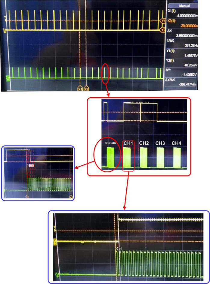
    To confirm the SPI communication has no problem, I have measured the signals on the SPI bus. So the question remains what I am overlooking and why I am getting 0x007FFFFF instead of the expected value for the mid-supply voltage.

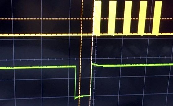
  • Also, the DRDY - CLCK lines:

  • Hello Kamen,

    Thanks for your updates.

    I'll start with the latest question. /DRDY will return high in line with the first SCLK falling edge. This is not an issue with the device. You must use the falling edge of /DRDY to monitor for new data.

    Your register settings appear correct to read the MVDD measurement. I'm not sure what the implications of the Reserved bits are (bits 6:5 in CONFIG3), but you should confirm that you are writing the correct values to be sure. It is not expected to see bit 5 read as '0'. Please note that you should be reading data with SPI settings as CPOL = 0 and CPHA = 1. Data is shifted out on the rising edge of SCLK, so your uP should be latching the data on the falling edge.

    Also, you mentioned that the test signal amplitude does not change when you select the 1x or 2x options in CONFIG2? It certainly should make a difference, can you please share those results? Again - confirm that you can read the correct register values back from the device to be sure the settings have taken effect.

    Best Regards,

  • Dear Ryan,
    Thanks for the notes - eventually I found a silly omission in the definitions of constants to configure registers (also seen in the code above). Now I believe I am able to get the mid-supply level correctly.

    Now I am dealing to see the test signal correctly - in fact I am seeing the pulses, just a bit confused how to translate them into voltage.

    First of all, checking the datasheet, I am not yet quite clear what should the test signal DC level be in theory?

    Kind regards,
    Kamen
  • Hi Kamen - the DC level of the test signal will be the offset voltage for that given channel. To translate the output code to volts, you will need to multiply the decimal equivalent by the LSB size. For more information, please read the Data Format section on page 38.

    Regards,

  • Hi Ryan,
    I think I am getting the correct signals&values now. Big thanks for the efforts and time you spent on answering my questions.
    Kind regards,
    Kamen
  • Hi Kamen,

    What you are doing is actually the correct way to translate the output code. In binary two's complement, you need to test the MSB to know the sign of the output. Essentially, for MSB = 0, you can convert the output code directly from hex to decimal to volts. When MSB = 1, you'll need to subtract (2^24 - 1) from the decimal code before converting to volts. You basically did the same thing (but in reverse order). Your result should be 4.7945V - 4.5V = -0.002549V.

    This DC level of -2.55mV is the offset voltage for that channel between INxP and INxN as seen at the output of the PGA stage.

    Best Regards,