This thread has been locked.

If you have a related question, please click the "Ask a related question" button in the top right corner. The newly created question will be automatically linked to this question.

ADS54J66: user data frame and a question about the use of LC and HC register

Part Number: ADS54J66

Hi,

Let me ask you a question as below about operating mode of ADS54J66.

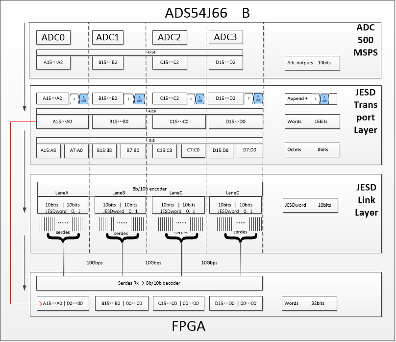
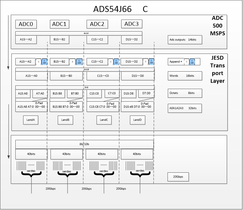
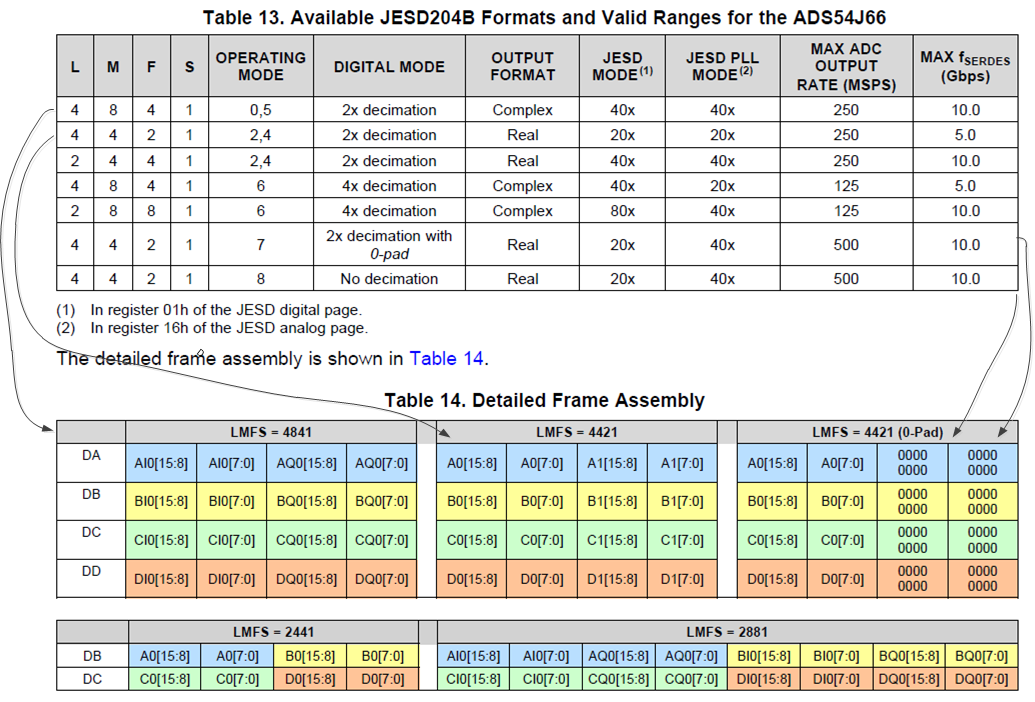
Q1) The data sheet describes below. (datasheet page38, table13 and table 14).

        is the line that i connect from the JESD MODE(up) to the frame assembly is the truth(especially the mode 8)?

Q2) in the mode 4421 (not the 4421 0-pad), there is a data named A1.

         is A1  the next sample data of A0?

Q3) in the datasheet, (datasheet page38, table 59).

what's the function of the LC register(low resolution counter value) and the HC register(high resolution counter value). 

Is it possible to use operating mode "8" (No decimation) in case LMF=244?

I suppose it is possible but let me confirm this to you for sure.

Thank you in advacne.

  • User,

    Q1. Yes

    Q2. A0 is the first sample for Channel A, A1 is the second sample for Channel A and so on.

    Q3. These will be removed from the data sheet. I have attached a preliminary draft of what we are currently working on. These are still

            shown in this draft but will be removed.

    Q4. No. You cannot operate mode 8 in LMF = 244.

    Regards,

    Jim

      SBAS745.pdf

  • JIm,

            your answer is very fit for me,  thank you first.

            And i have another question about the dataflow and its data format of this device( from adc to jesd204b( transport layer, link layer)). about this question, i a draw a data flow diagram.

            but it is a pity that i leave it in my company. so, i will upload it in tomorrow,  please comfirm it for me.

    Regards,

    qiu xu


  • Jim,

            I have another question about the ADS54J66's datasheet, it make me feel puzzled. About this data flow diagram question, i spend some time to draw some drafts to make my question more clear. there are be named "ADS54J66      A" , “ ADS54J66      B” , “ADS54J66      C”. I post them below.

             these question are related to the OPERATION MODE 8.

    Q1 > The three data flow diagrams below from ADC outputs data stream to the JESD204B output bit stream, which one is the correct understanding?

             If none of them is right, please help me confirm which one is closest to the right answer.

    Q2 > I tend to think that "ADS54J66      A" is right, but in the datasheet (page 38, table 14),  the subtable (named LMFS = 4421( 0-pad )) which is related to the operation mode 8, there are 16bits 0 fallow A0[15:8] A[7:0], i don't know these zeros come from where ?

             So i drawed the daft B and C.

    Q3 > About the “ ADS54J66      B”, i think may be the serdes Rx or the JESD204B Rx register is 32 bits ,so when they deal the 16bits data, they must append 16bits zeros. so i can ignor these zeros?

            So, when i desgin the FPGA receiver, i should also use a 32 bits register to get this data, and just ignor the low-16bits?

    Q4 > About the “ ADS54J66      C”,i also doubt its correctness, because it even use 20Gbps.

    Q5 > The red line in “ ADS54J66      B”, can i think the data at the ends of the red line are equal?

    Q6 > I want know, after the SERDES RX and JESD204B RX, the data i get in FPGA is the ADC output data append 0 and OVR. is this understanding the right?

  • maybe the operation mode use the  data frame assmebly LFMS=4421 in table 14 not the LMFS=4421 0-pad?

  • jim, 

            maybe the operation mode 8 use the  data frame assmebly LFMS=4421 in table 14 not the LMFS=4421 0-pad?

    Regards,

    qiu xu

  • User,

    That is correct. Mode 8 uses LMFS = 4421, no 0-padding.

    Regards,

    Jim

  • Jim,
    Thank you very much. I can solve the other question which i asked before.
    Regards,
    Jim
  • Jim,

            Sorry to disturb you agin.

            When i read the table 72(datasheet, page 69), there are two registers i don't know in this table.

    So, in the step 2, what are the use of register 4002h and register 4001h. I can not find the describtion of them.

    Regards,

    Qiu xu

  • Jim,
    I have another question about the table 72(datasheet, page 69). In the step 6, wirite 02h to register 6016h. But in table 70, it says that this register's 7-1 bit must be writed 0, and the LSB can be configed. And the 02h in binary should be 00000010, it is violate table 70.
    maybe there is a mistake in the table 70 either table 72?
    can you tell me, what's data shoule be writed in 6016h to config PLL mode 40x for channel A, B.
    Regards,
    Qiu xu
  • Jim,
    sorry to bother you agin, but this problem is really difficult.
    in table 27(datasheet page 29), the MSB of register 0053h, its name is CLK DIV. I know the function of this register, But i really don not know why i must set a input clock divider.
    for example, in operation mode 8, i would like input a 500Mhz clock to sample a 200Mhz sine signal. i don not know why i must divide it by 2 or 4 ?
    please spend a little time to answer it, thanks first.
    Regards,
    Jim
  • User,
    We are looking into this.
    Regards,
    Jim
  • 7776.SBAS745.pdfUser,

    Please use the preliminary updated data sheet attached. These registers you mentioned are not used. They will be removed on the next revision of the data sheet.

    Regards,

    Jim

  • User,

    Let me know if this is still an issue after you have looked at the updated data sheet I sent you.

    Regards,

    Jim

  • Jim,

            thank you for your updated datasheet. But it is pity that i find the next three question are shtill bother me. 

    Q1)  When i read the table 72(datasheet, page 69), there are two registers i don't know in this table.
            So, in the step 2, what are the use of register 4002h and register 4001h. I can not find the describtion of them.   they have no use and they will be remove?

    Q2)  I have another question about the table 72(datasheet, page 69). In the step 6, wirite 02h to register 6016h. But in table 70, it says that this register's 7-1 bit must be writed 0, and the LSB can be configed. And the 02h in binary should be 00000010, it is violate table 70. maybe there is a mistake in the table 70 either table 72?

            can you tell me, what's data shoule be writed in 6016h to config PLL mode 40x for channel A, B.

    Q3)  in table 27(datasheet page 29), the MSB of register 0053h, its name is CLK DIV. I know the function of this register, But i really don not know why i must set a input clock divider.
    for example, in operation mode 8, i would like input a 500Mhz clock to sample a 200Mhz sine signal. i don not know why i must divide it by 2 or 4 ?


    Regards,

    Qiu xu

  • User,

    In my last post I told you address 4002h and 4001H are not valid address's and are going to be removed from the data sheet.

    The ADS54J66 uses 2 interleaving cores per channel. So, the input clock should be divided by 2 to generate the sampling clock of interleaving cores.

    Therefore, in ADS54J66 we must always set the CLK DIV bit as 1.We probably will rename this bit for ADS54J66 as ‘ALWAYS WRITE 1’ to avoid any confusion to customer.

    For 40x mode, write a 0x02 to address 16h in page 6A00. There is an error in the data sheet.


    Regards,


    Jim

  • Jim,
    can i use this device to sample a signal which complex bandwidth is 250MHz or a sighal which bandwidth is 125Mhz.
    Regards,


    Qiuxu
  • User,

    Do you want to sample a complex input with a bandwidth of 250MHz or do you want a complex output of 250MHz bandwidth? What sample rate do you plan on using and what mode? The part is only rate for 200MHz complex output bandwidth when using the decimation modes and 245.76MHz when bypassing decimation and sampling at 500Msps. 

    Regards,

    Jim 

  • jim,

    Q1) so what's the meaning of this sentence(200-MHz Complex Bandwidth or 100-MHz Real Bandwidth Support , datasheet page 1)?

    Q2) this device's Maximum Clock Rate is 500 MSPS, so i want know, can i use this device to sample a signal which complex bandwidth is 240Mhz, in operation mode 0?

    Q3) no matter what operation mode is, this device only can  Support 200-MHz Complex Bandwidth or 100-MHz Real Bandwidth signal?

    Regards,

    QiuXu

  • User,

    The ADS54J66 uses 2 interleaving cores per channel. So, the input clock will always be divided by 2 to generate the sampling clock for the interleaving cores. Therefore, when using the ADS54J66, for master page 80h, register 0053h, the CLK DIV bit should always be set to 1. In the next revision of the data sheet, this bit will be specified as ‘ALWAYS WRITE 1’ to avoid any confusion to the customer.

    Regards,

    Jim

  • QiuXu,

    When using the device in mode 0 with complex output data (CHA = I data, CHB = Q data, CHC = I data, CHD = Q data), you can get a signal from +/-110MHz centered about Fs/4. This would only provide you with 2 channels of complex output data.

    In real mode, you can get up to 4 channels of output data, but the bandwidth will only be 110MHz bandwidth.

    If you are using the device in mode 0, with Fs = 500Msps, and if your input tone is at 240MHz, you would get a complex output at 115MHz. 

    For question 3, if you run in bypass mode, you can get real data bandwidth of 250MHz.

    Regards,

    Jim

  • JIM,

    thank you for your kind.

    Q1) in operation mode 0, with Fs = 488M, can i sample signal which Fo is 366M and bandwidth is 220M(FL = 256M, FH = 476M)?

    Q2) in operation mode 0, with Fs = 480M, can i sample signal which Fo is 360M and bandwidth is 210M(FL = 255M, FH = 465M)?

    Regards,

    QiuXu

  • Jim,

          thank you for your kind.

          i have not finded the ADC‘s required clock performance, so i have a question.

          now,  i want supply the ADS54J66 a clk signal(its phase noise performance parameter is 400Mhz -110DBc@1Khz).Is this clk can drive the ADC well?

          or  can you give me a tip, where i can find this parameter about the ADS54J66?

    Regards,

    QiuXu