This thread has been locked.

If you have a related question, please click the "Ask a related question" button in the top right corner. The newly created question will be automatically linked to this question.

DAC7551: Question on the serial write operation of DAC7551

Part Number: DAC7551
Hi. I would like to control DAC7551 with the SPI master of Microsemi IGLOO2 FPGA according to the serial write operation timing diagram (Figure 1) specified in the datasheet ( www.ti.com/lit/ds/symlink/dac7551.pdf ). It seems that the SDIN in Figure 1 of datasheet is shifted at the rising edge of SCLK. 

The voltage level of DAC7551 in my testing is specified as follows:

VDD =3.3V.  VREFH = 1.8V.   VREFL = 0V. 
GND = 0V.  CLR = 1.8V.   IOVDD = 1.8V.  
VOUT = VFB. (DAC7551 analog output)
 
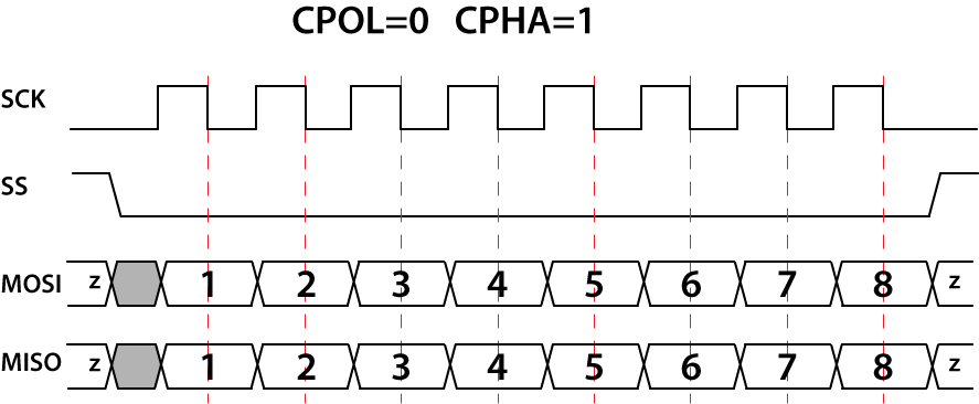
And here're the configuration of my SPI master according to the timing diagram in datasheet: 
1. Serial clock (SCLK) level is low when SPI is idle. 
2. Serial data input (SDIN) sampled at falling edge of SCLK and shifted at rising edge.
The measurement results on the oscilloscope are shown as follows, where yellow, blue and green waveform are VOUT, SDIN and SCLK of DAC7551, respectively. The SYNCn (Frame synchronization input) of DAC7551, which're not shown on oscilloscope, is pulled to logic level low 125 ns before the 1st cycle of SCLK and pulled back to logic high (3.3V) at the end of serial data transmission (i.e. last SCLK cycle).


Digital input code = 1023 (in binary expression: 0000_0001_1111_1111)
Inline image 1
Digital input code = 1024
Inline image 2
Digital input code = 2047
Inline image 3
Digital input code = 2049
Inline image 4
Digital input code = 4095
Inline image 5
My question is, since DAC7551 is a 12-bit DAC, the input code of 2048 should give a mid-level VOUT of approximately 900mV given VREFH = 1.8V. But in my measurement result, VOUT was 1.77V and 1.66V for 2047 and 2049 input codes, respectively. Also, when the input digital code was switched from 1023 to 1024, the VOUT jumped from 863mV to 419mV. Is my SPI configuration (SDIN shifted at rising edge of SCLK) correct for the serial data writing of DAC7551?
Thank you in advance for your patience, and please let me know if you need any information further. 

Best regards
  • Hi Johnson,

    Welcome to E2E and thank you for your query. I am not able to see the attached waveform. Looks like there is a shift in the bits in the SPI sequence. You can check the SCLK phase and polarity settings. If it still doesn't work, please attach the waveform - I will look into it.

    The value of CPOL should be 0 and CPHA should be 1 for correct operation.

    Regards,
    Uttam Sahu
    Applications Engineer, Precision DACs
  • Hi, Uttam. Thank you for your replying. The CPOL=0 & CPHA=1 setting should be in agreement with that in my SPI as described in my article:

    1. Serial clock (SCLK) level is low when SPI is idle.
    2. Serial data input (SDIN) sampled at falling edge of SCLK and shifted at rising edge.

    (See dlnware.com/.../spi_cpol0_cpha1.png)

    I've included waveform figures in my article. If you can't see the figure, would you mind to e-mail me so that I can attach the waveform to you?
    (tsai53@purdue.edu)

    Thank you again for your help

    Best
  • Hi Johnson,

    I couldn't open the link. Could you please use rich formatting and attach the file instead of the link?

    Regards,
    Uttam
  • Hi, Uttam. Here's the measurement result of DAC7551 serial writing operation on oscilloscope. Please let me know if you still can't see the attached figures. 
    --
    The configuration of my SPI master according to the timing diagram in DAC7551 datasheet is : 
    1. Serial clock (SCLK) level is low when SPI is idle. 
    2. Serial data input (SDIN) sampled at falling edge of SCLK and shifted at rising edge.
    The measurement results on the oscilloscope are shown as follows, where yellow, blue and green waveform are VOUT, SDIN and SCLK of DAC7551, respectively. The SYNCn (Frame synchronization input) of DAC7551, which're not shown on oscilloscope, is pulled to logic level low 125 ns before the 1st cycle of SCLK and pulled back to logic high (3.3V) at the end of serial data transmission (i.e. last SCLK cycle).


    Digital input code = 1023 (in binary expression: 0000_0001_1111_1111)
    Inline image 1
    Digital input code = 1024
    Inline image 2
    Digital input code = 2047
    Inline image 3
    Digital input code = 2049
    Inline image 4
    Digital input code = 4095
    Inline image 5
    My question is, since DAC7551 is a 12-bit DAC, the input code of 2048 should give a mid-level VOUT of approximately 900mV given VREFH = 1.8V. But in my measurement result, VOUT was 1.77V and 1.66V for 2047 and 2049 input codes, respectively. Also, when the input digital code was switched from 1023 to 1024, the VOUT jumped from 863mV to 419mV. Is my SPI configuration (SDIN shifted at rising edge of SCLK) correct for the serial data writing of DAC7551?
  • Hi Johnson,

    I am taking this over mail as you are facing some issue with the attachment.

    Regards,
    Uttam