Other Parts Discussed in Thread: ADS127L01
Hi there,
I have been struggling to acquire reasonable readings from the ADS127L01EVM using an external microcontroller. The board itself is operating excellently (and we are very happy with the performance characteristics) as we were able to test it with the TI Delta-Sigma ADC EvaluaTIon Software.
Now, we are trying to use an Arduino to communicate with the device via SPI and read a voltage.
Our hardware setup is as follows (Pin X refers to Arduino connections):
- CS is tied low by installing a jumper on J6[1].
- START pin, which is tied to DVDD, is tied to Pin 8 (set to OUTPUT) via TP21 (JP11 is uninstalled).
- JP5 is installed to power down Y1 and JP6[3] is tied to Pin 5 (set to OUTPUT). Pin 5 is configured on the Arduino to supply an 8MHz clock signal to the EVM board as per Section 5.6 in the datasheet.
- External 5V supply is connected to JP3[2] (supplied from the Arduino 5V pin).
- The external supply ground is shared with the EVM ground using one of the GND test points.
- On S3, HR=1, FORMAT = 0, OSR[1:0] = 00, FSMODE = 0, FILTER[0:1] = 01 as per Table 2 in the datasheet.
- The SPI port is connected to the corresponding SPI pins on the Arduino (MISO, MOSI, SCLK).
- The DRDY pin is connected to Pin 4 (set to INPUT).
When this setup is completed and the Arduino connected to power, the ADS127L01EVM lights up (so it seems things are connected properly).
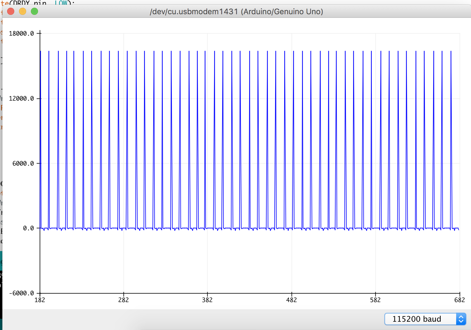
The difficulty comes when I upload my program to read conversion results. I connected a 3.3V DC voltage to the terminal block and I get this output:
What's good is that it looks like I'm clocking out data from the device, but what's bad is it's nonsense. The periodicity of the "spikes" looks like the problem could originate from the void loop() function in the Arduino program, but I'm unsure. I am returning unformatted data (not converting to voltage, hence the y-axis scale).
Here is my Arduino sketch:
#include <SPI.h>
#include <avr/io.h>
#include <util/delay.h>
//define constants
const int DRDY_pin = 4;
const int START_pin = 8;
const byte readCommand = 0b00010010; //RDATA command from Table 19. Command Definitions
const byte blank = 0b00000000;
SPISettings settingsA(16000000, MSBFIRST, SPI_MODE1); //1.6MHz SCLK, CPOL = 0, CPHA = 1)
void setup() {
pinMode(3, OUTPUT); // Output pin for OCR2B timer
pinMode(5, OUTPUT); // Output pin for OCR0B timer
// Set up the 8 MHz output
TCCR0A = bit(COM0A1) | bit(COM0B1) | bit(WGM01) | bit(WGM00);
TCCR0B = bit(WGM02) | bit(CS00);
OCR0A = 1;
OCR0B = 0;
//Setup SPI device
Serial.begin(115200);
pinMode (DRDY_pin, INPUT);
pinMode (START_pin, OUTPUT);
//Synchronization Timing (SPI Interface) as per Figure 85.
digitalWrite(DRDY_pin, LOW);
digitalWrite(START_pin, HIGH);
digitalWrite(START_pin, LOW); //in SPI interface mode, DRDY goes high as START is taken low (it's an active-low pin)
delayMicroseconds(4); //t_w(STL)
SPI.begin();
}
void loop() {
digitalWrite(START_pin, HIGH); //After START is returned high, DRDY stays high while the digital filter completes reset and settles
if(digitalRead(DRDY_pin) == LOW){ //After valid data are ready for retrieval, check for DRDY goes low
Serial.println(readADC(readCommand), 10); //Send readADC command, output with 10 significant figures.
//delayMicroseconds(10);
}
}
float readADC(byte primaryConfig){
noInterrupts(); //disable interrupts
SPI.beginTransaction(settingsA); // set settingsA
delayMicroseconds(5);
SPI.transfer(primaryConfig); // send read byte command
byte firstByte = SPI.transfer(0x00); // read the first byte
byte secondByte = SPI.transfer(0x00); // read the second byte
byte thirdByte = SPI.transfer(0x00); // read the third byte
interrupts(); //enable interrupts
int firstSixteenBits = (firstByte << 8) | secondByte;
int lastTwentyFourBits = (firstSixteenBits << 8) | thirdByte;
float valueDEC = (float(lastTwentyFourBits) * 5.00000) / 16777216.0000000; // convert into voltage using a reference of 5.0000V
float valueNOFORMAT = float(lastTwentyFourBits);
//return valueDEC;
return valueNOFORMAT;
SPI.endTransaction();
//delayMicroseconds(3);
}
This is the oscilloscope trace of the DIN/MOSI (1) and SCLK (2) lines. As can be seen, the RDATA command is sent, followed by 3 empty byte commands when the Arduino reads the DOUT line (not shown in the oscilloscope trace).
I have a few questions about all of this is:
- What is the correspondence between Figure 1. SPI Interface Timing, Figure 85. Synchronization Timing (SPI Interface), and Figure 91. SPI Keep-Out Time (tKO)? Are they to be interpreted simultaneously? Where does the DIN command come into play in Figure 91? To me, Figure 91 implies that you don't need to send any read commands at all since all you have to continually check the DRDY line.
- Does the START pin have to be raised high after each conversion?
- If I wanted to continuously sample an input voltage, do I just issue one start command and then follow Figure 91? Currently, I'm sending the start command at each loop iteration.
We will eventually use a Raspberry Pi for the end use of the ADC because we will need to use it at 512ksps (and the Arduino serial write speed limits us). Our first priority is just understanding the mechanics of how to communicate properly with the device and get the results we expect.
Your assistance is much appreciated.
Rohan Nuttall
Vancouver, Canada


