Other Parts Discussed in Thread: ADS1299
Hello,
I am working on a custom board with ADS1299-4. The board seems to be in a good shape, I succeed to collect an ECG signal, I am yet to collect EEG signal, though. However, I tried the device in several locations - in home environment the ECG data appeared right away, without any difficulties. I believe this is a proof that the device itself does not exhibit significant problems (e.g. disturbances caused by the power-supply converters on the board). In office, however, there were disturbances and it was impossible to see a signal even once. I am yet to investigate the nature of those disturbances and check if I can see some signal after filtering. I am willing, however, to be able to get useful signal in such a noisy environment. Therefore, I am trying to figure out what measures to take to suppressing the disturbance components:
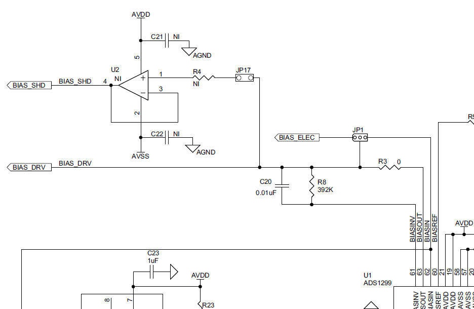
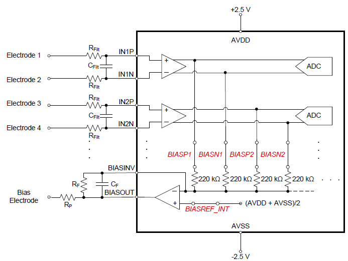
- when all channels are disabled, BIASOUT voltage is about 0.5Avdd. When a channel is enabled, however, BIASOUT voltage tries to reach AVdd. I believe, during normal operation BIASOUT voltage should not diverge much from 0.5Avdd, but having it approaching Avdd perhaps indicates that the common-mode disturbance is that large so the driver tries to compensate it but is unable... Could that be the case, is that large voltage at the BIASOUT output normal at all?
- perhaps shielding of electrode connecting wires is worth to try - however, as there is an option for active shielding in ADS1299EEG-FE, does it worth to try active shielding in the custom board? Could I expect any significant decrease of external disturbances in this case?
- I found interesting notes here https://github.com/lukaszmargielewski/EEG_BLE . Basically, that guy claims that an RLD driver without the feedback RC group could offer a great CMRR, and also, that in therms of avoiding the 50/60Hz mains disturbance, connecting the inverting input channel pins together to get a reference electrode is a better solution rather than using SRB1. Do these claims make sense, is it worth to try that?
Kind regards