This thread has been locked.

If you have a related question, please click the "Ask a related question" button in the top right corner. The newly created question will be automatically linked to this question.

ADS1292: single-ended input

Part Number: ADS1292
Other Parts Discussed in Thread: ADS1294, ADS1298, THS4551, THS4521, TINA-TI

Hello,

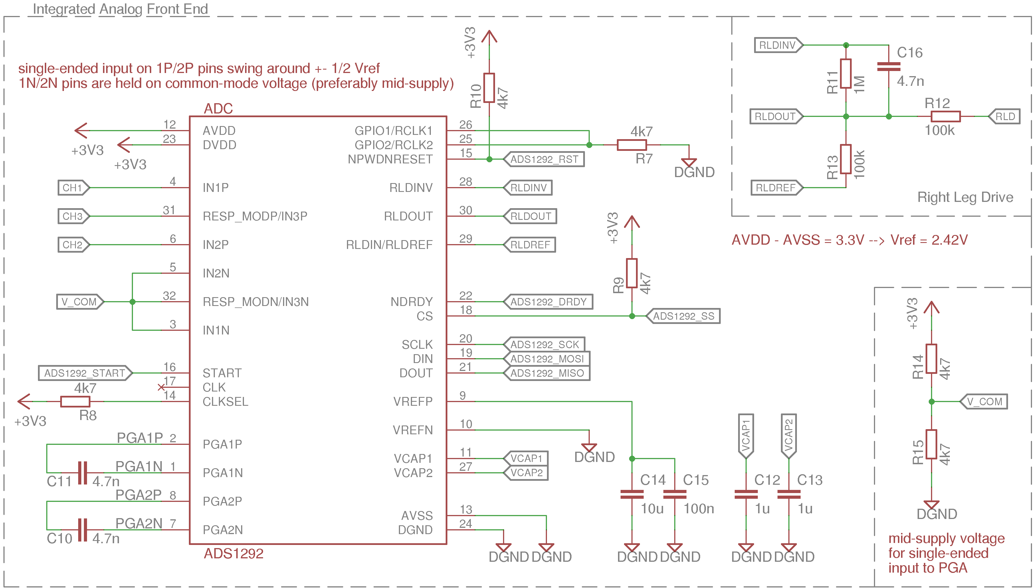
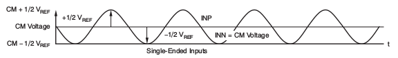
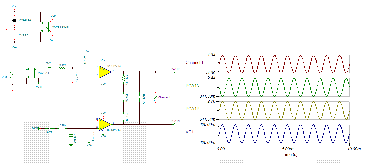
I'm using the ADS1292 for EMG signal acquisition. My circuit has filtering and amplification stages before feeding the signal into the ADS1292, so the input signal will be single-ended.  According to the data sheet differential input is recommended and I understand the advantages of doing that, but as it is not suitable in my application I need to go the other way. Means I drive the negative input INN to mid-supply using a voltage divider. I'm just wondering if my design is correct. I need to admit that I'm new to this field and I couldn't find appropriate answers to my problem in this forum.

1) is the circuit for the single-ended input correct like I do? Are there better ways to provide the mid-supply than using a voltage divider?

2) does it work together with the single voltage supply I provide? (AVDD = 3.3V , AVSS = 0V)

3) according to the data sheet, the RLDIN/RLDREF can also be used as single ended input. Is that a better way to go? But I still like to use the Right Leg Drive...

Thank you for your support

  • Hello Christoph,

    Thanks for your post and interest in our ADS1292.

    What you are describing is actually a pseudo-differential input configuration, where the negative inputs are actually driven to a common-mode voltage rather than shorted to ground. I believe this is an improved configuration if you do not care about the DC component of your input signal since you can now use the full-scale range of the ADC for better dynamic range.

    A resistor divider is certainly one approach to set the common-mode voltage on the INxN pins. This is exactly how it's done inside the ADS1292 to generate RLDREF. However, if you are enabling the RLDSENSx bits, the RLD amplifier output will also contain some inverted common-mode signal, which you do not want to connect directly to the INxN inputs. If all RLDSENSx bits are disabled, then RLDOUT will simply be a buffered mid-supply voltage, which you could use for VCOM.

    In your comments, you wrote "single-ended input on 1P/2P swing around +-1/2 Vref." I believe you should set the INxP common-mode voltage to mid-supply as well, not mid-reference (Vref / 2). The absolute voltage on each input pin is limited by the supplies, so centering them both around mid-supply gives you the maximum input voltage swing. Differentially, the input voltage is limited by the reference used by the ADC to make conversions. If INxP is centered around Vref / 2 and INxN is centered around mid-supply, you will create a DC offset in the measurement.

    Also, just to make sure you are aware, the ADS1292 only contains two simultaneously-sampling ADCs - the third auxiliary input (IN3P/IN3N) will have to be switched in to one of the channels through the MUX. Have you considered using our ADS1294? This device has better performance and very similar features and interface to the ADS1292.

    Best Regards,

  • First of all thank you very much for your support.

    Ryan Andrews said:
    What you are describing is actually a pseudo-differential input configuration, where the negative inputs are actually driven to a common-mode voltage rather than shorted to ground. I believe this is an improved configuration if you do not care about the DC component of your input signal since you can now use the full-scale range of the ADC for better dynamic range.

    Does this also imply that I should use AC coupling on the input signals?

    Ryan Andrews said:
    In your comments, you wrote "single-ended input on 1P/2P swing around +-1/2 Vref." I believe you should set the INxP common-mode voltage to mid-supply as well, not mid-reference (Vref / 2). The absolute voltage on each input pin is limited by the supplies, so centering them both around mid-supply gives you the maximum input voltage swing. Differentially, the input voltage is limited by the reference used by the ADC to make conversions. If INxP is centered around Vref / 2 and INxN is centered around mid-supply, you will create a DC offset in the measurement.

    I refer that comment to the information I found in the data sheet, but I also realize that I prefer having a higher input range, especially as I already amplify the signal in previous stages before I feed it into the ADS1292.

    According to this graphic the the input swings around common mode with +-1/2 Vref. So to increase the range I can set a higher Vref (4V) by increasing the analog supply to 5V. In this point I am not sure how to realize your suggestion. Can I configure mid-supply as common-mode voltage in the configuration registers (could not find it)? 

    Ryan Andrews said:
    Also, just to make sure you are aware, the ADS1292 only contains two simultaneously-sampling ADCs - the third auxiliary input (IN3P/IN3N) will have to be switched in to one of the channels through the MUX. Have you considered using our ADS1294? This device has better performance and very similar features and interface to the ADS1292.

    Thank your for the hint. I am aware that the third channel needs to be multiplexed in this case. Actually I will adapt the design using only 2 channels. The system I design is more a development kit at the moment, so 2 channels are enough. But I will also take a look at the ADS1294.

    Regards,

    Christoph

  • Hi Christoph,

    Since you have already done the work to level-shift your input signal, I don't think it would make much sense to AC couple the inputs. I believe AC coupling is more common when you are interfacing the sensor inputs directly to the chip without active filtering in between. Besides, you would still need to set the DC common-mode voltage at the inputs anyway to ensure that they remain within the limits of the ADS1292 PGA.

    Regarding the figure in the datasheet, I have to admit this is a typo. We do not specify what the "CM Voltage" is, but if you assume that both INP and INN are centered around the same voltage, then the difference between the two curves can actually range from -Vref to +Vref. This same figure is used in related product datasheets (i.e. ADS1298), but has since been updated to reflect this correction. Therefore, if you imagine that both inputs are centered around CM Voltage = mid-supply, then INP will be allowed to swing anywhere from AVDD to AVSS as long as it never exceeds INN by more than Vref.

    Sorry for the confusion, I hope this is more clear now.

    Best Regards,

  • Hello Ryan,

    Assumed I use Gain=1 with the PGA the input INP could swing CM +- Vref. If I interpret the data sheet correctly the input on the pins is also limited to AVSS - 0.3V to AVDD + 0.3V. So in my case with the unipolar supply my signal range on the input of INP would be -0.3V to 3.6V (which is not optimal for my application). So if I get your point about the mid-supply centering of the INP pin right... I could use e.g. a bipolar supply AVDD = +1.65V (mid-supply) and AVSS = -1.65V -- then theoretically the input range for the signal on INP would be -1.95 to 1.95 V, but then be shifted to a DC offset 1.65V because of the mid-supply on INN?

    Edit: I discovered another solution to my problem now. Wouldn't it be better to use a input driver like the THS4551 (single-ended input to differential output amplifier) or THS4521 to be able to use the ADS1292 in the recommended differential configuration? Is there any reason not to use this driver in front?

  • Hello Christoph,

    You are correct that the input pins of the device are limited by the analog supplies, though these are the Absolute Maximum Ratings. I don't recommend designing the application circuit to operate consistently at those limits. Why do you say this input range is not optimal for your design? Don't forget that the PGA gain is differential, and that the full-scale range of the ADC can still be achieved with a single-ended input to the PGA stage. As long as the DC common-mode voltage is fairly close on each input, the differential output should be centered near 0V. Increasing the gain also decreases the input-referred noise of the ADC itself. See the attached TINA-TI simulation circuit below as an example for PGA = 6:

    PGA_model_1CH.TSC

    The THS45xx family of full-differential amplifiers (FDAs) is great for level-shifting your input signal and converting it to a differential output in one stage. We often recommend those devices for our ADCs which do not have a high-impedance PGA input stage, but rather interface directly with the sampling network of the delta-sigma modulator. Since the ADS1292 does include a high-impedance input, I would think that a high-speed FDA would be overkill for this design. Not to mention, they tend to have a higher 1/f noise density curve than low-bandwidth precision amplifiers. Overall, I think this would diminish performance and add unwanted complexity and cost to your design.

    Best Regards,