Other Parts Discussed in Thread: DAC8830
I think there is a problem with the documentation for this converter in that whether CPAH=1 or CPAH=0 in regards to the SPI mode. If we go on ever reliable wikipedia we find the following information:
- At CPOL=0 the base value of the clock is zero, i.e. the idle state is 0 and active state is 1.
- For CPHA=0, data is captured on the clock's rising edge (low→high transition) and data is changed at the falling edge (high→low transition).
- For CPHA=1, data is captured on the clock's falling edge (high→low transition) and data is changed at the rising edge (low→high transition).
- At CPOL=1 the base value of the clock is one (inversion of CPOL=0), i.e. the idle state is 1 and active state is 0.
- For CPHA=0, data is captured on the clock's falling edge (high→low transition) and data is changed at the rising edge (low→high transition).
- For CPHA=1, data is captured on the clock's rising edge (low→high transition) and data is changed at the falling edge (high→low transition).
And:
| SPI Mode | Clock Polarity (CPOL/CKP) | Clock Phase (CPHA) | Clock Edge (CKE/NCPHA) |
|---|---|---|---|
| 0 | 0 | 0 | 1 |
| 1 | 0 | 1 | 0 |
| 2 | 1 | 0 | 1 |
| 3 | 1 | 1 | 0 |
When looking at the data sheet for the ADS127L01 we see the following:
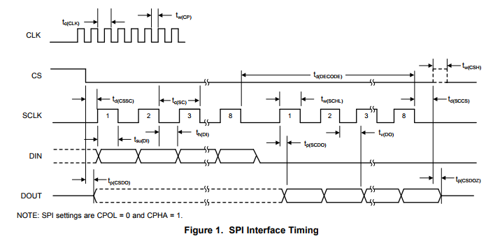
Which although stating CPHA = 1 the timing diagram is consistent with CPHA = 0 as data is changing on the rising edge and been latched on the falling edge (Page 12). Furthermore in the text it is stated "Only SPI mode 1 (CPOL = 0, CPHA = 1) is supported". I have used this ADC before with a TI MCU where I used (TivaC):
SSIConfigSetExpClk(SSI0_BASE, SysCtlClockGet(), SSI_FRF_MOTO_MODE_1, SSI_MODE_MASTER, 20000000, 16);
So I would guess that the error is the timing diagrams? or I am in someway confused? I do have my development system with the MCU still but I would probably have to do quite a lot of fiddling to get reliable results on this due to the large phase shifts in that system (flying leads).
James.