This thread has been locked.

If you have a related question, please click the "Ask a related question" button in the top right corner. The newly created question will be automatically linked to this question.

ADC32RF45EVM: Frequency-dependent power loss

Part Number: ADC32RF45EVM
Other Parts Discussed in Thread: ADC32RF45

Description:

I see a larger than expected frequency-dependent power loss across the bandwidth of the ADC.  I’m referring to loss from signal input power at the SMA connector on the EVM board to the ADC output signal.  I would like an explanation from TI regarding how much of this loss is attributed to both the PCB and the ADC.

Hardware setup:

  • System setup from EVM Quick Startup Guide was followed closely
  • ADC32RF45 placed in Bypass LMFS82820 Mode
  • ADC Sampling frequency = 2949.12 MHz
  • 2nd Nyquist Zone operation
  • ADC Fs signal creation:  sig-gen à BP Filter à Splitter à LMK Ref & ADC Clock
  • Input signal creation:  sig-gen à BP Filter à Splitter à Spectrum Analyzer & ADC Input Ch. A
  • EVM Configuration Files:  “LMK_ ADC32RF45_LMF_82820_ExtClock.cfg” and “ADC32RF4x_12bit_LMFS_82820.cfg”

Test 1: 

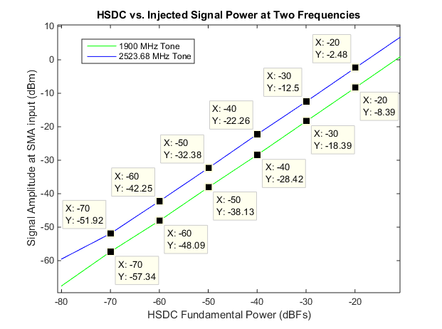
In this test, I selected two frequencies as input signals and swept the input power level.  I selected 1900 MHz because it was the recommended frequency in the EVM Quick Startup Guide.  The second frequency (2523.68 MHz) was selected because it was the same offset from the center of the band as 1900 MHz.  The X-axis shows the power levels as reported by the HSDC software while the Y-axis represents the measured signal input to the EVM board.  Over these measurements, a mean of approximately 6 dB in signal level change seen between these two frequencies.

Test 2: 

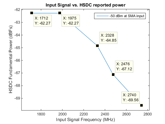
In this test, five frequencies (1712 MHz, 1975 MHz, 2328 MHz, 2476 MHz, and 2740 MHz) were chosen such that the entire instantaneous bandwidth of the ADC was covered while ensuring that none of the main spurs (interleaving or nth order) overlap.  The injected signal amplitude into the SMA connector was set to be -50 dBm for each test frequency.  The X-axis represents the input signal frequency while the Y-axis shows the fundamental power level reported by HSDC.  The plot shows a 7.29 dB roll-off in ADC power over the frequency range tested.

  • Hi,

    I suspect the differences would be attributable to several things across the frequency band you are looking at.

    First, the pass band of the baluns on the EVM will not be quite flat.  Some datasheets for baluns and transformers will have a nice plot showing the rolloff as you get towards the low or high end of their passband while others just have tables.   The ETC1-1-13 balun used on this EVM has 1GHz for its -1dB max corner and 2GHz for its -2dB max corner and then at 3GHz its listed at -3.5dB.   Multiple that by two as we have back to back baluns on the EVM, and you are operating in the range where the balun may be rolling off.  

    Second, the input impedance of the ADC analog input is not flat with frequency, and the nominal 50ohm internal termination listed for the device is effectively not flat considering parasitics.  So there may be some frequency dependent loss in getting the expected waveform at the input pins of the ADC.   That effect really made itself visible when driving the ADC with a diff amp that had some series resistance at the amp outputs - the series elements with the effective ADC impedance made a frequency-dependent voltage divider.   Driving from a 50ohm source through the baluns would probably still show some effect of imperfect impedance matching across frequency. 

    On my apps bench since I usually have a bandpass filter after the sig gen, the variability in the bandpass filters means that I am always adjusting the sign gen amplitude anyway for each frequency.  So I don't usually see these individual effects, but I also see some nonlinearity in the output of the sig gen as well.

    To really evaluate the flatness of the ADC itself I think you would have to measure the actual amplitude of the signal at the ADC pins with a diff probe of adequate bandwidth and compare that to the reported amplitude of the fundamental.  I don't see a flatness spec for the ADC itself in the datasheet for the device. 

    Regards,

    Richard P.

  • I understand that part of the loss is due to the balun stages and some of it due to the ADC. I was hoping you had more data pertaining to this from either your EVM PCB testing or simulations. I am a bit surprised that there is nothing in the ADC spec on this. Figure 64 shows the transfer function for the input pins, but doesn't include the ADC itself. I am putting this part on a new PCB and am looking for any information to get the best performance I can out of the part.

    Lastly, I just want to make clear that I adjusted the signal generator to drive the same power level (-50 dBm) into the EVM board SMA for every frequency. I did not probe the PCB after the baluns, however.

    Thanks, Shawn B.