Because of the holidays, TI E2E™ design support forum responses will be delayed from Dec. 25 through Jan. 2. Thank you for your patience.

This thread has been locked.

If you have a related question, please click the "Ask a related question" button in the top right corner. The newly created question will be automatically linked to this question.

ADS1220: Data Conversion at Specific Timings

Part Number: ADS1220
Other Parts Discussed in Thread: MSP430FR4133, XTR117, , ADS1247, ADS124S06

Hello TI,

This is my first post on this forum. I already have successfully designed Flowmeter electronic Instrument(using MSP430FR4133) for displaying live flow rate and Cumulative total on a dual line customize segment LCD (4-Mux). It is meter mounted unit with inputs as magnetic sinusoidal pick-off and REED switch through turbine flow meter. With having 2-wire 4/20mA pulse output, 4-20mA analog o/p (XTR117) loop powered as well as battery powered (just using 40µA when there is no loop supply available). It was all possible due to your great reference designs. We are very thankful for this.

Now I am designing a Electromagnetic flow meter indicator. In this coils will be excited using pulsed dc excitation(Constant Current) method. When a conductive fluid passes through the line, due to alternating magnetic field developed by the coils, voltage will induce at electrodes. In case of no flow or turbulence, the differential voltage across electrodes will be almost zero. 

I'm planning to use ADS1220 ADC converter IC for collecting differential voltage samples through stainless steel electrodes. 

The frequency of the pulsed dc excitation will be in the multiple of AC line frequency(50 Hz in India) for noise suppression. For most of our popular line sizes of flow meter, 6.25Hz shall be appropriate excitation frequency.

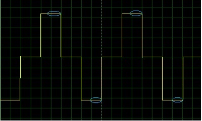
Below is the image of the pulsed dc excitation of the coils(timings generated by the same Micro-controller (MSP430FR4133, which is also a master to ADS1220). It is required to take samples of the electrode's signal at the instance highlighted with blue ovals in the below image.

I'll be using Simultaneous 50-Hz and 60-Hz rejection FIR filter config.

Now the questions about ADS1220 ADC are, how should I configure the ADS1220?

1. Should I use single shot mode or the continuous conversion mode?

2. What Should be the data rate?

3. Or single shot mode with 20SPS data rate? Should this work?

It would have been very helpful if TI could have given a reference design for Electromagnetic Flow Meter as well. :(

Regards,

Harish


  • Hi Harish,

    Welcome to the forum! There are several considerations relative to power, startup, and settling.  You also want to have your results to be consistent within the measurement window.  You could use single-shot mode at 20sps, but the problem is having confidence in the timing and that the input has adequately settled when starting the measurement.

    I would use a faster data rate, and capture a number of readings and average the results.  This way you can analyze the data as it is being captured to make sure the results have settled and are not influenced by the settling.  I would also use continuous conversion mode and end each measurement cycle with the POWERDOWN command to conserve power.  Conversion for the measurement cycle can start with the START/SYNC command.  Whether you use single-shot or continuous modes and which data rates you choose is really dependent on the level of confidence you have of the measurement itself.  If you should find that 20sps in single-shot mode also includes some analog settling, then you try adjusting the timing but this is inconclusive as there is not enough data for verification.  That is why I suggested multiple readings.

    To maintain consistency I would use a timer interrupt to start each cycle, with additional timers set to trigger various other events including sending of the START/SYNC command and POWERDOWN for each 1/2 cycle.

    Best regards,

    Bob B

  • Hi Bob,

    Thanks for your quick response.

    Bob Benjamin said:

    If you should find that 20sps in single-shot mode also includes some analog settling, then you try adjusting the timing but this is inconclusive as there is not enough data for verification.

    I'll be using turbine flow meter installed in the same line for the reference of flow velocity.

    The signal generated by the electrodes is generally having sensitivity of 150 µVolts/mps to 200µVolts/mps. (MPS is flow velocity in meter/sec). So, at a range of 0.5m/s to 15m/s differential signal generated by the electrodes generally lies in the range of 80µVolt to 5mVolt. The electronics will be powered by AC power (100V to 260V, 50Hz). This electrode's signal is very weak and highly prone to noise generated by AC power line frequency.

    That is why I was thinking to use 50Hz rejection filter setting of ADS1220. But, as per the datasheet I can not go beyond 20SPS if I use 50Hz rejection.

    If I use 5Hz biphasic pulsed dc excitation of the coils then I'll get 100ms ON time in either direction. Then sending START command after 50ms of rising edge of excitation pulse of coils(using 20SPS, 50Hz rejection & Some PGA gain ~16) and taking averages of some other samples. Should this work?

    Although I'll try with faster data rates too.

    As I'll be using inbuilt SMPS in the unit for power, so spending few mAmps will not bother me.

    Another question, can I measure negative samples too when using only unipolar analog power supply to ADS1220?

    Regards,

    Harish

  • Hi Harish,

    You can certainly try measuring the way you describe, and then you can compare the results with turbine flow meter. 

    You can measure differential signals with a unipolar supply as long as the common-mode input range requirements are met.  If your input (AINN or AINP) relative to AGND goes below AGND, then you would need a bipolar supply for the ADS1220.

    Best regards,

    Bob B

  • Hey Bob,

    Is there any possibility to take out the internal reference voltage at any pin of ADS1220? I need it for the reference of Instrumentation amplifier I'm using.

    Pin description of AD8220ARMZ says,

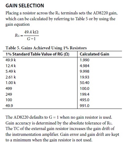
    Gain selection can be done by,

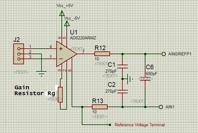
    The configuration in which AD8220ARMZ to be used(Gain typically between 10 to 20) is given below. J2 connects the electrode's raw signal.

    As adding precision low temperature drift shunt voltage reference will add cost in my project.

    If there is no way pulling out the internal reference 2.048V to any pin of ADS1220, iff comfortable, can you suggest me an alternate JFET instrumentation amplifier(low cost) that can serve the same purpose. if yes, a circuit with component value will be more helpful.

    Thanks & Regards,

    Harish

  • Hi Harish,

    Unfortunately the ADS1220 design does not allow for the internal reference to come out of the device.  We do have other ADCs with reference out capability, such as the ADS1247 (similar to the ADS1220) or the ADS124S06.  For the INA, the reference level is used to shift the output into the required input range of the ADC.  This should be a low noise source as this voltage will go directly into the ADC.  I'm sure TI has an equivalent INA device but unfortunately I'm not that familiar with the INA portfolio.  You could ask a similar request on the Amplifier forum under Precision Amplifiers.

    Best regards,

    Bob B

  • Hi Bob,

    I'm trying to communicate with ADS1220 with the library given by you with some modifications to use with MSP430FR4133.

    MSP430FR4133                    ADS1220

    P1.1  <<--------------------------  MISO (DOUT) 

    P1.0  >>--------------------------  MOSI (DIN) 

    P1.2  >>--------------------------  SCLK 

    P1.4  <<--------------------------  INT(DRDY) 

    P1.3  >>--------------------------  CS

    When I writes the gain to the configuration registers of ADS1220, reading back from that register returns me proper values. That means configuration of ADS1220 is good.

    But when I try to read the ADC value on AINP as AIN0 & AINN as AVSS, it just gives me 0xFFFFFFFF. Unfortunately I do have only dual channel scope, so can't monitor all pins simultaneously. I have tried reading ADC value in various configurations but no luck.

    //main.c file
    
    #include <msp430fr4133.h>
    #include "lcdLib.h"
    #include "ADS1220.h"
    
    // Global variable
    float Volt=1.23456;
    char buffer[15];
    char dFlag = 0, intr=9;
    
    void initGpio(void);
    void Init_Clock(void);
    void ConfigTimer(void);
    void SPIinit(void);
    void Init_StartUp(void);
    
    
    void main(void)
    {
    signed long tData=0;
    
        WDTCTL = WDTPW + WDTHOLD; // Stop Watchdog
        delay_ms(10); //Delay for power-on settling
        Init_StartUp();
        ADS1220SendResetCommand();
        ADS1220Init(); // Initializes the SPI port pins as well as control
        ADS1220Config(); // Set base configuration for ADS1x20 device
        ADS1220SetGain(ADS1220_GAIN_32);
        lcdInit(); // Initialize LCD
    
        while(1)
        {
    
    if (dFlag==1) // if new data is available
    {
    lcdClear();
    tData = ADS1220ReadData(); // get the data from the ADS1220
    ADS1220SendShutdownCommand();
    dFlag=0;
    Volt = (tData/2^23)*2.048;
    }
    ftoa(Volt,buffer,3);
    lcdSetText(buffer,0,0);
    
    intr=ADS1220GetGain();
    lcdSetInt(intr,14,1);
    
    
        } 
    }
    void initGpio(void)
    {
    P1DIR = 0xFF;
    P2DIR = 0xFF; P3DIR = 0xFF; P4DIR = 0xFF;
    P5DIR = 0xFF; P6DIR = 0xFF; P7DIR = 0xFF; P8DIR = 0xFF;
    P1REN = 0xFF;
    P2REN = 0xFF; P3REN = 0xFF; P4REN = 0xFF;
    P5REN = 0xFF; P6REN = 0xFF; P7REN = 0xFF; P8REN = 0xFF;
    P1OUT = 0x00;
    P2OUT = 0x00; P3OUT = 0x00; P4OUT = 0x00;
    P5OUT = 0x00; P6OUT = 0x00; P7OUT = 0x00; P8OUT = 0x00;
    // Disable the GPIO power-on default high-impedance mode
    // to activate previously configured port settings
    PM5CTL0 &= ~LOCKLPM5;
    }
    void ConfigTimer(void)
    {
        TA0CCTL0 |= CCIE;                                   // TACCR0 interrupt enabled
        TA0CCR0 = 3276;      //=32767/75 for 75Hz
        TA0CTL = TASSEL__ACLK | MC__UP;             // SMCLK, UP mode
    }
    
    void Init_Clock(void)
    {
    P4SEL0 |= BIT1 | BIT2;                  // set XT1 pin as second function
    
       do
       {
           CSCTL7 &= ~(XT1OFFG | DCOFFG);      // Clear XT1 and DCO fault flag
           SFRIFG1 &= ~OFIFG;
       } while (SFRIFG1 & OFIFG);              // Test oscillator fault flag
    
          __bis_SR_register(SCG0);                // disable FLL
        CSCTL3 |= SELREF__XT1CLK;               // Set XT1CLK as FLL reference source
        CSCTL0 = 0;                             // clear DCO and MOD registers
        CSCTL1 &= ~(DCORSEL_7);                 // Clear DCO frequency select bits first
        CSCTL1 |= DCORSEL_3;                    // Set DCO = 8MHz
        CSCTL2 = FLLD_0 + 243;                  // DCODIV = 8MHz
        __delay_cycles(3);
        __bic_SR_register(SCG0);                // enable FLL
        while(CSCTL7 & (FLLUNLOCK0 | FLLUNLOCK1)); // Poll until FLL is locked
    
        CSCTL4 = SELMS__DCOCLKDIV | SELA__XT1CLK; // set default REFO(~32768Hz) as ACLK source, ACLK = 32768Hz
                                                // default DCODIV as MCLK and SMCLK source
    
        PM5CTL0 &= ~LOCKLPM5;                   // Disable the GPIO power-on default high-impedance mode
                                                // to activate previously configured port settings
    }
    // Sets the USCI SPI peripheral to use A0
    void SPIinit(void)
    {
    UCA0CTLW0 |= UCSWRST;                     // **Put state machine in reset*
    UCA0CTLW0 |= UCMST | UCSYNC | UCMSB; // SPI master, synchronous
    UCA0CTLW0 |= UCSSEL_2 | UCSWRST; // Use SMCLK for bit rate clock and keep in reset
    UCA0BR0 = 4; // SMCLK/4 = SCLK (2MHz)
    UCA0BR1 = 0;
    UCA0MCTLW = 0;                            // No modulation
    UCA0CTLW0 &= ~UCSWRST; // Release peripheral for use
    }
    
    void Init_StartUp(void)
    {
        __disable_interrupt();               // Disable global interrupts
    
        initGpio();                        // Init ports (do first ports because clocks do change ports)
        //SetVCore(3);                         // USB core requires the VCore set to 1.8 volt, independ of CPU clock frequency
        Init_Clock();
        ConfigTimer();
        SPIinit();
    
        __enable_interrupt();                // enable global interrupts
    }
    
    #pragma vector = PORT1_VECTOR
    __interrupt void Port_1(void)
    {
    
    switch(__even_in_range(P1IV,16))
    {
    case 0: break;
    case 10:
    dFlag=1;
    break;
    default:break;
    }
    }
    
    //end of main.c
    //Changes made in ADS1220.c..
    
    void ADS1220Init(void)
    {
    
    P1SEL0 |= ADS1220_DIN | ADS1220_DOUT | ADS1220_SCLK ; //Set as secondary function
    P1SEL0 &= ~(ADS1220_DRDY | ADS1220_CS) ; //Set as GPIO pins
    
    // define initial states
    P1OUT |= ADS1220_CS; // CS is really 'not' CS, so it should be disabled high
    
    // define inputs
    P1DIR &= ~(ADS1220_DRDY); // DRDY is an input to the micro
    P1IES |= ADS1220_DRDY; // and should be used as an interrupt to retrieve data
    // define outputs
    P1DIR |= ADS1220_CS;
    
    return;
    
    }
    
    // ADS1220 Initial Configuration
    void ADS1220Config(void)
    {
    unsigned Temp;
    
    ADS1220ReadRegister(ADS1220_0_REGISTER, 0x01, &Temp);
    
    // clear prev value;
    Temp &= 0x0f;
    Temp |= ADS1220_MUX_0_G; //Input multiplexer configuration: 1000 : AINP = AIN0, AINN = AVSS
    
    // write the register value containing the new value back to the ADS
    ADS1220WriteRegister(ADS1220_0_REGISTER, 0x01, &Temp);
    
    ADS1220ReadRegister(ADS1220_1_REGISTER, 0x01, &Temp);
    
    // clear prev DataRate code;
    Temp &= 0x1f;
    Temp |= (ADS1220_DR_600 + ADS1220_CC); // Set default start mode to 600sps and continuous conversions
    //Temp |= (ADS1220_DR_600);
    //Temp &= ~(ADS1220_CC); // Set default start mode to 20sps and single shot conversions
    // write the register value containing the new value back to the ADS
    ADS1220WriteRegister(ADS1220_1_REGISTER, 0x01, &Temp);
    
    
    }
    /* Polling Function */
    int ADS1220WaitForDataReady(int Timeout)
    {
    if (Timeout > 0)
    {
    // wait for /DRDY = 1
    while (!(P1IN & ADS1220_DRDY) && (Timeout-- >= 0))
    ;
    // wait for /DRDY = 0
    while ( (P1IN & ADS1220_DRDY) && (Timeout-- >= 0))
    ;
    if (Timeout < 0)
    return 0; //ADS1220_TIMEOUT_WARNING;
    }
    else
    {
    // wait for /DRDY = 1
    while (!(P1IN & ADS1220_DRDY))
    ;
    // wait for /DRDY = 0
    while ( (P1IN & ADS1220_DRDY))
    ;
    }
    return ADS1220_NO_ERROR;
    }
    
    void ADS1220AssertCS( int fAssert)
    {
    if (fAssert)
    P1OUT &= ~(ADS1220_CS); 
    else
    P1OUT |= (ADS1220_CS); 
    
    }

    //Changes made in ADS1220.h

    // P1.3 #define ADS1220_CS BIT3 // P1.0 #define ADS1220_DIN BIT0 // P1.1 #define ADS1220_DOUT BIT1 // P1.4 #define ADS1220_DRDY BIT4 // P1.2 #define ADS1220_SCLK BIT2

    lcdLib.c
    #include "lcdLib.h"
    
    #define	LOWNIB(x)	P3OUT = (P3OUT & 0xF0) + (x & 0x0F)
    
    void lcdInit() {
    	delay_ms(100);
    	// Wait for 100ms after power is applied.
    
    	P3DIR = EN + RS + DATA;  // Make pins outputs
            P3SEL0 = 0x00;
    	P3OUT = 0x03;  // Start LCD (send 0x03)
    
    	lcdTriggerEN(); // Send 0x03 3 times at 5ms then 100 us
    	delay_ms(5);
    	lcdTriggerEN();
    	delay_ms(5);
    	lcdTriggerEN();
    	delay_ms(5);
    
    	P3OUT = 0x02; // Switch to 4-bit mode
    	lcdTriggerEN();
    	delay_ms(5);
    
    	lcdWriteCmd(0x28); // 4-bit, 2 line, 5x8
    	lcdWriteCmd(0x08); // Instruction Flow
    	lcdWriteCmd(0x01); // Clear LCD
    	lcdWriteCmd(0x06); // Auto-Increment
    	lcdWriteCmd(0x0C); // Display On, No blink
    }
    
    void lcdTriggerEN() {
    	P3OUT |= EN;
    	P3OUT &= ~EN;
    }
    
    void lcdWriteData(unsigned char data) {
    	P3OUT |= RS; // Set RS to Data
    	LOWNIB(data >> 4); // Upper nibble
    	lcdTriggerEN();
    	LOWNIB(data); // Lower nibble
    	lcdTriggerEN();
    	delay_us(50); // Delay > 47 us
    }
    
    void lcdWriteCmd(unsigned char cmd) {
    	P3OUT &= ~RS; // Set RS to Data
    	LOWNIB(cmd >> 4); // Upper nibble
    	lcdTriggerEN();
    	LOWNIB(cmd); // Lower nibble
    	lcdTriggerEN();
    	delay_ms(5); // Delay > 1.5ms
    }
    
    void lcdSetText(char* text, int x, int y) {
    	int i;
    	if (x < 16) {
    		x |= 0x80; // Set LCD for first line write
    		switch (y){
    		case 1:
    			x |= 0x40; // Set LCD for second line write
    			break;
    		case 2:
    			x |= 0x60; // Set LCD for first line write reverse
    			break;
    		case 3:
    			x |= 0x20; // Set LCD for second line write reverse
    			break;
    		}
    		lcdWriteCmd(x);
    	}
    	i = 0;
    
    	while (text[i] != '\0') {
    		lcdWriteData(text[i]);
    		i++;
    	}
    }
    
    void lcdSetInt(int val, int x, int y){
    	char number_string[16];
    	sprintf(number_string, "%d", val); // Convert the integer to character string
    	lcdSetText(number_string, x, y);
    }
    
    void lcdClear() {
    	lcdWriteCmd(CLEAR);
    }
    
    //////Display Float values
    void reverse(char *str, int len)
    {
        int i=0, j=len-1, temp;
        while (i<j)
        {
            temp = str[i];
            str[i] = str[j];
            str[j] = temp;
            i++; j--;
        }
    }
     
     // Converts a given integer x to string str[].  d is the number
     // of digits required in output. If d is more than the number
     // of digits in x, then 0s are added at the beginning.
    int intToStr(int x, char str[], int d)
    {
        int i = 0;
        while (x)
        {
            str[i++] = (x%10) + '0';
            x = x/10;
        }
     
        // If number of digits required is more, then
        // add 0s at the beginning
        while (i < d)
            str[i++] = '0';
     
        reverse(str, i);
        str[i] = '\0';
        return i;
    }
     
    // Converts a floating point number to string.
    void ftoa(float n, char *res, int afterpoint)
    {
        // Extract integer part
        int ipart = (int)n;
     
        // Extract floating part
        float fpart = n - (float)ipart;
     
        // convert integer part to string
        int i = intToStr(ipart, res, 0);
     
        // check for display option after point
        if (afterpoint != 0)
        {
            res[i] = '.';  // add dot
     
            // Get the value of fraction part upto given no.
            // of points after dot. The third parameter is needed
            // to handle cases like 233.007
            fpart = fpart * pow(10, afterpoint);
     
            intToStr((int)fpart, res + i + 1, afterpoint);
        }
    }
    

    lcdLib.h

    The ADS1220 breakout board's layout that I'm using.

    I'm really stuck into this.

    Thanks & Regards,

    Harish

  • Hi Harish,

    Are you sure your interrupt is working on DRDY?  I ask, because I do not see anywhere that you give the START/SYNC command.  You issue what I think is a POWERDOWN command (ADS1220SendShutdownCommand()), and to start conversions you need the START/SYNC command to START a new conversion if in single-shot mode, to start the initial conversion in continuous mode or anytime if in POWERDOWN mode when you want a new conversion.

    Best regards,

    Bob B

  • Hi Bob,

    Bob Benjamin said:

    You issue what I think is a POWERDOWN command (ADS1220SendShutdownCommand()), and to start conversions you need the START/SYNC command to START a new conversion if in single-shot mode, to start the initial conversion in continuous mode or anytime if in POWERDOWN mode when you want a new conversion.

    Thanks for pointing out. I've tried with the following but no luck this time either. (600SPS, Continuous Conversion)
    //main.c file
    
    #include <msp430fr4133.h>
    #include "lcdLib.h"
    #include "ADS1220.h"
    
    // Global variable
    float Volt=1.23456;
    char buffer[15];
    char dFlag = 0, intr=9;
    
    void initGpio(void);
    void Init_Clock(void);
    void ConfigTimer(void);
    void SPIinit(void);
    void Init_StartUp(void);
    
    
    void main(void)
    {
    signed long tData=0;
    
        WDTCTL = WDTPW + WDTHOLD; // Stop Watchdog
        delay_ms(10); //Delay for power-on settling
        Init_StartUp();
        ADS1220SendResetCommand();
        ADS1220Init(); // Initializes the SPI port pins as well as control
        ADS1220Config(); // Set base configuration for ADS1x20 device
        ADS1220SetGain(ADS1220_GAIN_32);
        lcdInit(); // Initialize LCD
        ADS1220SendStartCommand();  //To start the the first conversion
    
        while(1)
        {
    if (dFlag==1) // if new data is available
    {
    lcdClear();
    tData = ADS1220ReadData(); // get the data from the ADS1220
    dFlag=0;
    Volt = (tData/2^23)*2.048;
    }
    ftoa(Volt,buffer,3);
    lcdSetText(buffer,0,0);
    
    intr=ADS1220GetGain();
    lcdSetInt(intr,14,1);
    
    
        } 
    }
    void initGpio(void)
    {
    P1DIR = 0xFF;
    P2DIR = 0xFF; P3DIR = 0xFF; P4DIR = 0xFF;
    P5DIR = 0xFF; P6DIR = 0xFF; P7DIR = 0xFF; P8DIR = 0xFF;
    P1REN = 0xFF;
    P2REN = 0xFF; P3REN = 0xFF; P4REN = 0xFF;
    P5REN = 0xFF; P6REN = 0xFF; P7REN = 0xFF; P8REN = 0xFF;
    P1OUT = 0x00;
    P2OUT = 0x00; P3OUT = 0x00; P4OUT = 0x00;
    P5OUT = 0x00; P6OUT = 0x00; P7OUT = 0x00; P8OUT = 0x00;
    // Disable the GPIO power-on default high-impedance mode
    // to activate previously configured port settings
    PM5CTL0 &= ~LOCKLPM5;
    }
    void Init_Clock(void)
    {
    P4SEL0 |= BIT1 | BIT2;                  // set XT1 pin as second function
    
       do
       {
           CSCTL7 &= ~(XT1OFFG | DCOFFG);      // Clear XT1 and DCO fault flag
           SFRIFG1 &= ~OFIFG;
       } while (SFRIFG1 & OFIFG);              // Test oscillator fault flag
    
          __bis_SR_register(SCG0);                // disable FLL
        CSCTL3 |= SELREF__XT1CLK;               // Set XT1CLK as FLL reference source
        CSCTL0 = 0;                             // clear DCO and MOD registers
        CSCTL1 &= ~(DCORSEL_7);                 // Clear DCO frequency select bits first
        CSCTL1 |= DCORSEL_3;                    // Set DCO = 8MHz
        CSCTL2 = FLLD_0 + 243;                  // DCODIV = 8MHz
        __delay_cycles(3);
        __bic_SR_register(SCG0);                // enable FLL
        while(CSCTL7 & (FLLUNLOCK0 | FLLUNLOCK1)); // Poll until FLL is locked
    
        CSCTL4 = SELMS__DCOCLKDIV | SELA__XT1CLK; // set default REFO(~32768Hz) as ACLK source, ACLK = 32768Hz
                                                // default DCODIV as MCLK and SMCLK source
    
        PM5CTL0 &= ~LOCKLPM5;                   // Disable the GPIO power-on default high-impedance mode
                                                // to activate previously configured port settings
    }
    // Sets the USCI SPI peripheral to use A0
    void SPIinit(void)
    {
    UCA0CTLW0 |= UCSWRST;                     // **Put state machine in reset*
    UCA0CTLW0 |= UCMST | UCSYNC | UCMSB; // SPI master, synchronous
    UCA0CTLW0 |= UCSSEL_2 | UCSWRST; // Use SMCLK for bit rate clock and keep in reset
    UCA0BR0 = 4; // SMCLK/4 = SCLK (2MHz)
    UCA0BR1 = 0;
    UCA0MCTLW = 0;                            // No modulation
    UCA0CTLW0 &= ~UCSWRST; // Release peripheral for use
    }
    
    void Init_StartUp(void)
    {
        __disable_interrupt();               // Disable global interrupts
    
        initGpio();                        // Init ports (do first ports because clocks do change ports)
        //SetVCore(3);                         // USB core requires the VCore set to 1.8 volt, independ of CPU clock frequency
        Init_Clock();
        SPIinit();
    
        __enable_interrupt();                // enable global interrupts
    }
    
    #pragma vector = PORT1_VECTOR
    __interrupt void Port_1(void)
    {
    
    switch(__even_in_range(P1IV,16))
    {
    case 0: break;
    case 10:
    dFlag=1;
    break;
    default:break;
    }
    }
    
    //end of main.c

    Also, as you said the interrupt is not working at all because dFlag never sets.

    Thanks & Regards,

    Harish

  • Hi Harish,

    First make sure that DRDY is actually toggling by verifying with a scope.  If DRDY is toggling, and you don't get an interrupt, then you need to verify your settings and connections for the interrupt.  Sometimes it helps to clear the interrupt in case the interrupt was issued but never serviced previously.

    Best regards,

    Bob B

  • Hi Bob,

    Thanks for your continuous support.

    The DRDY interrupt was not enabled. I just enabled the DYDY pin interrupt and fixed it. Now it is working with the single shot conversion, 330SPS & Gain=1. The formula I'm using to convert to milli-volts is

    mVolt = (float)(tData/2^23)/2048;

    1. But now the problem is, when I use some PGA gain setting, it does not return the proper values. For Gain=16 I'm using the formula as,

    mVolt = (float)(tData/2^23)/128;

    The main.c file is attached below. Please suggest.

    0820.main.c
    #include <msp430fr4133.h>
    #include "lcdLib.h"
    #include "ADS1220.h"
    
    // Global variable
    float Volt=1.23456;
    char buffer[32];
    signed long tData=0;
    
    void initGpio(void);
    void Init_Clock(void);
    void SPIinit(void);
    void Init_StartUp(void);
    void ConfigTimer(void);
    
    
    void main(void)
    {
    
        WDTCTL = WDTPW + WDTHOLD;			// Stop Watchdog
        delay_ms(10);                               // Power-on settling time
        Init_StartUp();
        lcdInit();				        // Initialize LCD
        ADS1220Init();				// Initializes the SPI port pins as well as control
        ADS1220Config();				// Set base configuration for ADS1x20 device
        ADS1220SetGain(ADS1220_GAIN_16);
        //ADS1220Set50_60Rejection(0x10);		// Set ADS1220_REJECT_BOTH
        P7OUT &= ~BIT0;
        P7DIR |= BIT0;
        P7OUT &= ~BIT1;
        P7DIR |= BIT1;
    
    __bis_SR_register(LPM3_bits | GIE);     // Enter LPM3, enable interrupt
    
    }
    void initGpio(void)
    {
    	P1DIR = 0xFF;
    	P2DIR = 0xFF; P3DIR = 0xFF; P4DIR = 0xFF;
    	P5DIR = 0xFF; P6DIR = 0xFF; P7DIR = 0xFF; P8DIR = 0xFF;
    	P1REN = 0xFF;
    	P2REN = 0xFF; P3REN = 0xFF; P4REN = 0xFF;
    	P5REN = 0xFF; P6REN = 0xFF; P7REN = 0xFF; P8REN = 0xFF;
    	P1OUT = 0x00;
    	P2OUT = 0x00; P3OUT = 0x00; P4OUT = 0x00;
    	P5OUT = 0x00; P6OUT = 0x00; P7OUT = 0x00; P8OUT = 0x00;
    	// Disable the GPIO power-on default high-impedance mode
    	// to activate previously configured port settings
    	PM5CTL0 &= ~LOCKLPM5;
    }
    
    void Init_Clock(void)
    {
    	P4SEL0 |= BIT1 | BIT2;                      // set XT1 pin as second function
    	    do
    	    {
    	        CSCTL7 &= ~(XT1OFFG | DCOFFG);      // Clear XT1 and DCO fault flag
    	        SFRIFG1 &= ~OFIFG;
    	    } while (SFRIFG1 & OFIFG);              // Test oscillator fault flag
    
          __bis_SR_register(SCG0);              // disable FLL
        CSCTL3 |= SELREF__XT1CLK;               // Set XT1CLK as FLL reference source
        CSCTL0 = 0;                             // clear DCO and MOD registers
        CSCTL1 &= ~(DCORSEL_7);                 // Clear DCO frequency select bits first
        CSCTL1 |= DCORSEL_3;                    // Set DCO = 8MHz
        CSCTL2 = FLLD_0 + 243;                  // DCODIV = 8MHz
        __delay_cycles(3);
        __bic_SR_register(SCG0);                // enable FLL
        while(CSCTL7 & (FLLUNLOCK0 | FLLUNLOCK1)); // Poll until FLL is locked
    
        CSCTL4 = SELMS__DCOCLKDIV | SELA__XT1CLK; // set default REFO(~32768Hz) as ACLK source, ACLK = 32768Hz
                                                  // default DCODIV as MCLK and SMCLK source
    
        PM5CTL0 &= ~LOCKLPM5;                     // Disable the GPIO power-on default high-impedance mode                                           // to activate previously configured port settings
    }
    
    void ConfigTimer(void)
    {
        TA0CCTL0 |= CCIE;                           // TACCR0 interrupt enabled
        TA0CCR0 = 16384;                            // 0.5 sec delay
        TA0CTL = TASSEL__ACLK | MC__UP;             // ACLK, UP mode
    }
    // Timer A0 interrupt service routine
    #pragma vector = TIMER0_A0_VECTOR
    __interrupt void Timer_A (void)
    {
    		lcdClear();
    		Volt = (float)(tData/2^24)/128;    // FSR for Gain=16 will be 0.128V
    		ftoa(Volt,buffer,4);
    		lcdSetText(buffer,0,0);
    		ADS1220SendStartCommand();
    
    }
    // Sets the USCI SPI peripheral to use A0
    void SPIinit(void)
    {
    	UCA0CTLW0 |= UCSWRST;                     // **Put state machine in reset*
    	UCA0CTLW0 |= UCMST | UCSYNC | UCMSB;			// SPI master, synchronous
    	UCA0CTLW0 |= UCSSEL_2 | UCSWRST;				// Use SMCLK for bit rate clock and keep in reset
    	UCA0BR0 = 4;								// SMCLK/4 = SCLK (2MHz)
    	UCA0BR1 = 0;
    	UCA0CTLW0 &= ~UCSWRST; 						// Release peripheral for use
    }
    
    void Init_StartUp(void)
    {
        __disable_interrupt();             // Disable global interrupts
    
        initGpio();                        // Init ports (do first ports because clocks do change ports)
        Init_Clock();
        SPIinit();
        ConfigTimer();
    
        __enable_interrupt();              // enable global interrupts
    }
    
    #pragma vector = PORT1_VECTOR
    __interrupt void Port_1(void)
    {
    	if(P1IFG & BIT4)
    	{
    		tData = ADS1220ReadData();	// Get the data from the ADS1220
    		P1IFG &= ~BIT4;
    		ADS1220SendShutdownCommand();
    	}
    
    
    }

    2. Another problem I faced is when I compile the same code with CCS, it generates around 14Kb code size. But when I compile with IAR, it generates only 5.3Kb size. IS there any settings with the linker. I'm using CCS version 6.2.0.

    Thanks & Regards,

    Harish

  • Hi Harish,

    When you have applied gain, are you certain that the input voltage is within the proper common-mode input range for the ADS1220?  What is the voltage you are applying and what output code do you get prior to any conversion?  This would be very helpful to know in helping to diagnose your issues.

    As far as the code size, this larger code size is often due to the debugger code.  Try changing the configuration to Release.  When using the Release build, you can no longer use the debugger.

    Best regards,

    Bob B