Hi folks,
we have four ADS127L01 in a daisy-chain configuration:
- SCLK, MOSI, nCS: common for all chips
- START: common for all chips
- DRDY: OR-ed together and routed to a microprocessor
- DAISYIN: grounded on the last chip, connected to DOUT of the previous chip on the others
- DOUT: connected to DAISYIN on the following chip (and to the microprocessor's MISO from the first chip
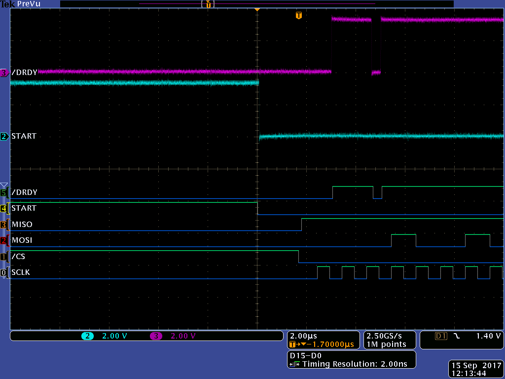
The chips' configuration is LP, OSR 128, Wideband 1 filter, results are read using the SPI mode. On the following figure, there is an overview of the MCU-ADC interface behaviour:

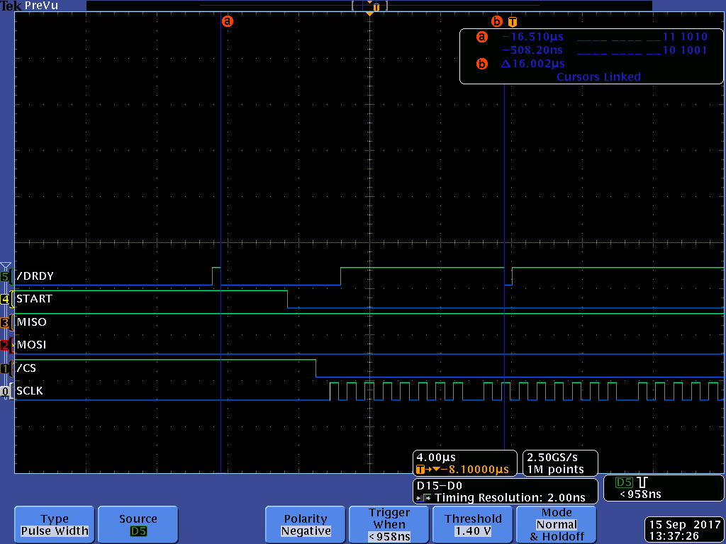
The first two readings are successfull (all CRCs are correct), but on the last one, the data are corrupted (and further reading is stopped by the SW). The following figure shows a detailed view of reading #1…

…and the last figure shows a detailed view of reading #3:

The only difference I can spot is, that
- on correct readings, the DRDY pulse after CS activation is either not present at all or is present before the first data bit is shifted out
- on erroneous readings, the DRDY pulse is present after shifting out the first data bit.
Questions:
1. Do we handle the DRDY signal correctly (the OR-ing)?
2. What is the purpose of DRDY pulsing?
3. What means the negative DRDY pulse after CS activation - when START is low?
Thanks for ideas
Jan