I have a design with three TI ADC’s two ADS8861IDGS and one ADS8860IDGS as we have two differential channels and one single-ended. All three share their SCLK and SDO lines and have switchable ConvST and DIN lines. The problem I have is that on power-up all three devices are outputting on SDO, this means that we have to connect all three devices and run through a sampling single cycle, at which point they all release the SDO line. This behaviour is very frustrating and is not stated in the datasheet.
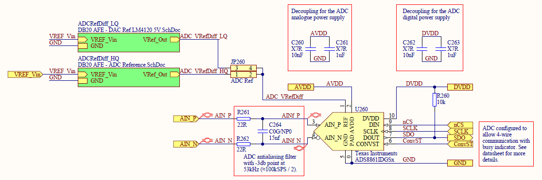
I have included the schematic below. VRef is 5V, AVDD is 5V and DVDD is 3V3. On power-up ConvST is pulled to GND and SDO & DIN (nCS) are pulled to DVDD, all with 10k resistors. Would anyone be able to take a look at this and tell me if I should be doing something differently to make the devices power up with SDO high impedance?