This thread has been locked.

If you have a related question, please click the "Ask a related question" button in the top right corner. The newly created question will be automatically linked to this question.

ADS1675: Needs a Low-Jitter, 5V clock

Part Number: ADS1675

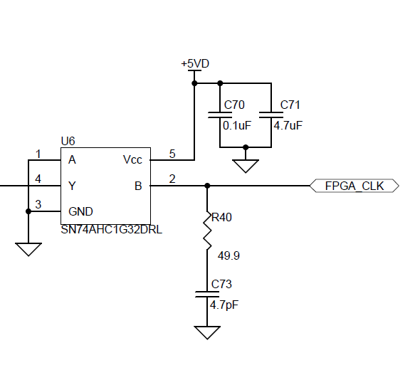
Hi, I'm designing a product using TI's ADS1675 and note in the datasheet that the conversion clock for this IC needs to have amplitude equal to AVdd, which is typically 5V (and will be 5V in this design). Since this is a precision application we need a super-low jitter clock, and when I research those parts, all the parts are available in 3.3Vdd or less. Most clock sources with 5V output are legacy devices with unacceptably poor jitter.

What does TI recommend for a super-low jitter 5V clock source? I would be happy to use a logic level translator as long as I can find one with super low injected jitter... although many level translators are not specified for this quantity, so it's not easy finding one. Are there any solid recommendations? 

Thanks for reading,

Graham 

  • Hello Graham,

    Thanks for your interest in our ADS1675, and please excuse my delay.

    Have you taken a look at the clock circuit used in the ADS1675REF design? We used the FPGA PLL followed by a level translator to generate the ADS1675 clock input. This will broaden the range of crystal oscillators you can choose from.

    ADS1675REF Clock input:

    The max clock jitter that you can tolerate really depends on the max input signal frequency and the desired SNR. For a delta-sigma ADC, the best-case SNR while considering only clock jitter can be estimated by:

    SNR = 20*log(2*pi*fIN*tJITTER) + 10*log(OSR)

    Use the highest input signal frequency you wish to measure in your system and set SNR equal to the typical SNR spec for the ADC. The OSR (oversampling ratio) will be determined by the DRATE setting.This will approximate how much jitter the ADC can tolerate before the SNR is degraded below the typical performance spec.

    Best Regards,