A related question is a question created from another question. When the related question is created, it will be automatically linked to the original question.
If you have a related question, please click the "Ask a related question" button in the top right corner. The newly created question will be automatically linked to this question.
ADS8691: Reading ADC port through SPI Communication
Can you give us more information about the issue you have? what's your input signal and your conversion code? so we can see how not accurate,also more information about your design and test:
Are you using internal or external voltage reference?
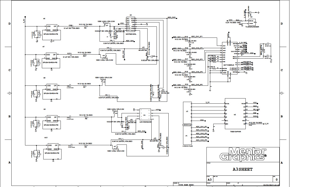
Can you upload your schematic?
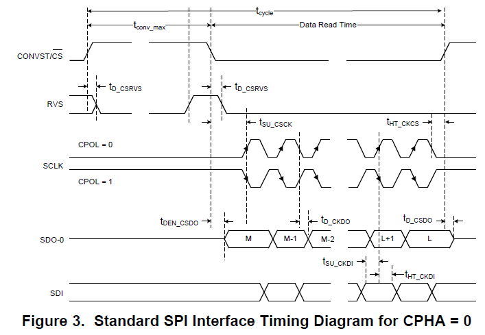
Your timing for digital bus(SCLK, SDO and CONVST) captured with a scope
Your schematic shows that you are using AD7193 from ADI which is a 24-bit 4 differential/8 pseudo differential input sigma-delta (Σ-Δ) ADC, it's not a schematic for our ADS8691, can you please double check?
Hi Sarathi, I apologize for missing your post. From your schematic, you should get the data if your timing is correct and even the data is not accurate: 1. Please capture your digital timing for CONVST/SCLK/SDI/SDO and upload the screenshot for check. 2. A balanced input RC is recommended in ADC input, please refer to the schematic in ADS8681EVM user guide. Even ADS8691 has integrated AFE, it's better to have a buffer before ADS8691 to isolate the input with your another ADC(MAX11200, our apps expert from Delta-Sigma team can give your best suggestion for the replacement). 3. A reset pulse signal is recommended on /RST pin after power up ADS8691, do not connect it to 5V supply directly with a pull-up resistor. 4. Please disconnect the input with MAX11200 and front-end circuit, use one DC voltage signal as input to ADS8691 for test purpose. Please let me know the result after your implement these suggestions, thanks.
I am working with your suggestions. Now I had done changes in the schematic. Beginning I was working in ADS8691 EVM. During power-up, some configuration is done.
Can you please tell me the configuration need to be done in software while booting up
I suggest you to test according to two steps as below:
Firstly, don't change input range, test directly by applying a DC signal on ADC's input after power up (default configurations: ±3 × VREF and internal Voltage reference), check if conversion code is correct with ±3 × VREF range. If the code is correct, this means that your timing also hardware connection are correct and ADC is working well.
Secondly, change input range to 1.5 × VREF according to the command as below:
Data frame: <11010_10><000010100><00000000><00001011>
Then, by applying a same DC voltage on ADC input (make sure the signal is in the range), check if conversion code is correct with 1.5 × VREF range. If yes, this means that your register programming is successful.
Remark: use Half-word write command: 11010_10_<9-bit address>_ <16-bit data> With this command, only the LS byte of the 16-bit data word is written at the specified register address.
Please let me know your result, thanks.
By the way, we don't have ADS8691EVM which is 18-bit version in same family, I suppose you are trying to test on ADS8681EVM, this command can be used for ADS8681, but you can't test ADS8691 by replacing ADS8681 on this EVM board, just let you know.
I tried as per your suggestion, I am unable to receive any data in the SD0 pin.
I am using master as Raspberry pi 3 board - bcm2835 Library.
From the master board, I need to read the ADC port of ads8691.
I did all the configurations which are listed below:
Reset power control register (Bitorders mentioned in 0 - 7 direction)
Initialization - 0xD000, 0x05, 0x00, 0x69 (To enable write of 5-0 Bits of Reset power control register)
Write - 0xD000, 0x04, 0x00, 0x0C ( Active mode(0), Disable NAP mode of Converter(0), PoR(0),Reserved(0), Input
alarm disabled(1), VDD alarm disabled(0), Reserved (00))
SDI Control register - 0xD000, 0x08, 0x00, 0x00 (CPOL = 0, CPHASE = 0, Reserved (000000)
SDO Control register - 0xD000, 0x0C, 0x00, 0x02 (Same protocol followed for SDI (00), 0000 (Reserved), 1(Internal clock),
0(Reserved))
Data out control register - 0xD000, 0x10, 0x00, 0x08 (000(Value output is the conversion data),1(Two parity bit are appended to the
LSB's of the output data) ,0000(Reserved))
Range selection register - 0xD000, 0x14, 0x00, 0x00 (0000(+/- 3 x Vref),00(Reserved), 0(Internal reference is enabled), reserved(0))
Before configuration Reset pin made low followed by 1000ms delay and again made High. (Done in program)
I didn't expect you programmed internal registers directly. As suggested above, firstly we should make sure your ADC is working and you can get correct conversion data after power up ADC, nothing should be programmed after power up ADC and only one reset signal is desired on /RST pin after power up, by default, input range is ±3 × VREF, internal reference is used,1-bit SDO mode, Standard SPI with CPOL = 0 and CPHASE = 0. Please work on this and check your timing with a scope as below including RVS signal, also check if your conversion code is correct with these default configurations.
Please note that 32 are expected within a data transfer frame. Please let me know your result with this test. Thanks.