This thread has been locked.

If you have a related question, please click the "Ask a related question" button in the top right corner. The newly created question will be automatically linked to this question.

ADC12J4000EVM: Problems with jesd204b interface

Part Number: ADC12J4000EVM
Other Parts Discussed in Thread: ADC12J4000, ADC12DJ3200, LMX2581, LMK04828

Hello!

I'v got adc12j4000EVM rev.E3 and I try to connect it to my vcu108 xilinx board. Bypass mode 3760 Msps.

According the datasheet for this ADC I am using following parameters for jesd(xilinx jesd 204b ip core v7.1) - for default parameters from adc gui:

F=8

K=4

L=8

LineRate = 7.52Gbps

ReferenceClock = 188MHz

SYSREF on Positive Edge

Using global clock 1

scrambling on

sysref always on

sysref required on re-sync

In additional transceiver control ports I'v changed polarity for gt_rx ports; In ADC gui v1.1 I press button "program clock" in bypass mode; And for test I am turning on Short/Long transport test.

So I expect to see rx_frame_error bus all zeros and the sequence on output bus.

But I have infrequent errors. What may be the reason of such problem.

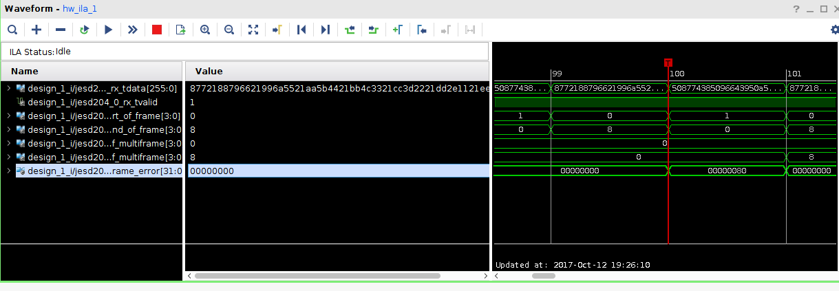
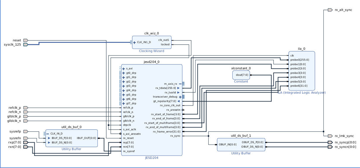
(block design and chip scope print in attachment)

  • Hi Al

    My documentation from Xilinx indicates that for 7520 Mbit/sec lane rate the Ref Clk should be Lane_rate/20 = 376MHz and the Core Clk should be Lane_rate/40 = 188 MHz.

    Does reducing the ADC clock rate and resulting lane rate change the behavior? If so then the issue may be due to signal integrity issues in the high speed data interface.

    If not, and if the errors only occur once in a while, then the issue may be due to incomplete handling of JESD204B alignment monitoring characters which are inserted into the ADC12J4000 output data stream in compliance with the standard. Please refer to section 5.3.3.4 of the JESD204B standard.

    You may also be interested in this firmware developed to interface the ADC12DJ3200 with the KCU105.

    http://www.ti.com/lit/zip/slvc698

    This firmware will be similar to what is needed for the ADC12J4000 with VCU108. (detailed sample mapping and FPGA target are different, other aspects are very similar).

    Best regards,

    Jim B

  • As I can see in your example there is Line Rate 6000Mbit/sec and Ref clk = Line_Rate/40 = 150 MHz...
    Thank you for this example I'l try to do the same with my configs.
  • I'v tried your example it leads the same result. Only one difference(besides constraints, line rate etc) in Vivado2017.1 I can't drive tx(rx)_core_clk with rxoutclk because there is an error:

    [DRC REQP-1740] GTx R/TXOUTCLK drives invalid load: GTHE3_CHANNEL cell design_1_i/jesd204_phy_0/inst/jesd204_phy_block_i/design_1_jesd204_phy_0_0_gt_i/inst/gen_gtwizard_gthe3_top.design_1_jesd204_phy_0_0_gt_gtwizard_gthe3_inst/gen_gtwizard_gthe3.gen_channel_container[0].gen_enabled_channel.gthe3_channel_wrapper_inst/channel_inst/gthe3_channel_gen.gen_gthe3_channel_inst[0].GTHE3_CHANNEL_PRIM_INST pin design_1_i/jesd204_phy_0/inst/jesd204_phy_block_i/design_1_jesd204_phy_0_0_gt_i/inst/gen_gtwizard_gthe3_top.design_1_jesd204_phy_0_0_gt_gtwizard_gthe3_inst/gen_gtwizard_gthe3.gen_channel_container[0].gen_enabled_channel.gthe3_channel_wrapper_inst/channel_inst/gthe3_channel_gen.gen_gthe3_channel_inst[0].GTHE3_CHANNEL_PRIM_INST/RXOUTCLK (net: design_1_i/jesd204_phy_0/inst/jesd204_phy_block_i/design_1_jesd204_phy_0_0_gt_i/inst/gen_gtwizard_gthe3_top.design_1_jesd204_phy_0_0_gt_gtwizard_gthe3_inst/gen_gtwizard_gthe3.gen_channel_container[0].gen_enabled_channel.gthe3_channel_wrapper_inst/channel_inst/rxoutclk_out[0]) should only drive a BUFG_GT load, but drives one or more invalid loads such as FDRE cell design_1_i/ila_0/inst/ila_core_inst/trace_data_ack_reg[0]. Please insert a BUFG_GT between the GT and its load(s).

    So I drive it by refclk_mon from iobufs_ti module(is that correct?)
    Iam using only 2 xilinx IP cores without any my algorithms, so I think may be it is a problem in EVM GUI or hardware? Is there any known issues of this board?

    I'v done more tests: there is no errors if I choose "on-board Fs Selection" = 3100Msps bypass mode and rare errors if 3500Msps bypass mode

  • I think I understand where is the problem:
    there is LMK04828BISQ/NOPB chip on my board www.ti.com/.../snas605ar.pdf - max frequency is 3080
    MHz and gui configuration tries 3760 Msps. So I'v got correct data on 3100 Msps and lower and got errors on higher Line rate

    Am I right that maximum line rate for this board is 3100Msps?

  • Hi Al

    It should be possible to get the EVM to work at 3760MSPS with your capture board, but the required clocking setup changes can cause an increase in Fs/2-Fin spur and therefore reduced SFDR performance.

    To operate at clock rates above 3100MHz the following changes must be made:

    1. LMX2581 output divider configuration is changed so the clock sent to the LMK04828 is 1/2 of the clock rate sent to the ADC.
    2. LMK04828 divider settings are reduced by a factor of 2 to account for the lower rate input clock.

    The standard ADC12J4000EVM GUI settings already incorporate these changes when Fclk is set above 3100 MHz. If you are using the standard EVM GUI as your starting point, you can load those settings and then make the additional changes necessary to create the reference clock frequency needed by the Xilinx FPGA (rather than the Altera FPGA in the TI capture board).

    The spur performance degrades due to crosstalk between the two outputs of the LMX2581. Some energy from the CLK/2 output couples into the CLK output send to the ADC. This results in the ADC CLK having energy at both CLK and CLK/2 which creates the timing relating sampling spur at Fs/2-Fin.

    An alternative solution to achieve better performance would be to acquire one of the production ADC12J4000EVM (Rev A) that use a different clocking design which is capable of operation up to 4 GHz clock rate. That design has no issues with crosstalk or reduced SFDR performance at high clock rates.

    Best regards,

    Jim B

  • Thank you for your reply. But I still don't understand the reason of my problem. I'v tried Ref Clk = Lane_rate/20 = 376MHz and Core Clk = Lane_rate/40 = 188 MHz as written here www.ti.com/.../slau580b.pdf section 6.3. And I still got the same errors, also I'v tried to change pre-emphasis strength from EVM GUI: when it is hight errors becomes more frequent but no one value clears this errors at all.

  • Hi Al

    Have you made any progress on this?

    Your calculated Ref Clk and Core Clk frequencies are correct but you may not be updating the dividers as needed.

    When the EVM is configured for ADC CLK frequencies above 3100 MHz, the clock sent to the LMK04828 is running at 1/2 the frequency of the ADC clock. For your case the LMK04828 clock will be at 3760/2 = 1880 MHz. The LMK dividers need to be configured for that input frequency, so the dividers are 5 and 10, not 10 and 20 as you might expect.

    Best regards,

    Jim B

  • Hi Jim

    Now I am working at 3100, I'v already tried changing dividers if you talking about this:

    1. Go to LMK04828 address 0x110 and enter a “5” in the write data box and click the Write Register
    button.
    2. Click the Read Register button and verify a “5” is read back.
    3. Go to address 0x100, do a Read Register and verify the value “A” is read back. If not, write this value
    to this address.

    This is from http://www.ti.com/lit/ug/slau580b/slau580b.pdf

    It doesn't help.

  • Hi Al
    I'm not sure what else to try.
    FPGA reference/core clock rate and SERDES signal pre-emphasis are the only items that should need to be adjusted for the higher line rate mode of the EVM.
    Best regards,
    Jim B
  • Hi Jim!

    I also tried rev.A and got the same result...

    I'v done the same steps:

    1)set jumper kc705 jtag

    2)press Program clock 4000 Msps in adc12j4000evm gui

    3)lmk reg 0x110 set to 5 from gui

    4)program vcu108

    Parameters of my jesd block:

    default sysref always = sysref always off

    scrambling on

    F 8

    K 4

    default sysref required on re-sync => sysref not required

    Line rate 8Gbps

    Ref clock 400MHz

    PLL type Cpll

    Block design is:

    in additional control transceiver ports gt_rxpolarity = 255(change all lanes polarity)

    constraints:

    set_property PACKAGE_PIN R9 [get_ports refclk_p]

    set_property PACKAGE_PIN AY9 [get_ports glblclk_p]
    set_property IOSTANDARD LVDS [get_ports glblclk_p]

    set_property PACKAGE_PIN K2 [get_ports {rxp[0]}]
    set_property PACKAGE_PIN H2 [get_ports {rxp[1]}]
    set_property PACKAGE_PIN F2 [get_ports {rxp[2]}]
    set_property PACKAGE_PIN D2 [get_ports {rxp[3]}]
    set_property PACKAGE_PIN T2 [get_ports {rxp[4]}]
    set_property PACKAGE_PIN R4 [get_ports {rxp[5]}]
    set_property PACKAGE_PIN P2 [get_ports {rxp[6]}]
    set_property PACKAGE_PIN M2 [get_ports {rxp[7]}]

    # sync's
    set_property -dict {PACKAGE_PIN BF10 IOSTANDARD LVDS} [get_ports rx_syncp]
    set_property PACKAGE_PIN AJ13 [get_ports rx_alt_sync]
    set_property IOSTANDARD LVCMOS18 [get_ports rx_alt_sync]

    set_property PACKAGE_PIN K14 [get_ports rx_lmk_sync]
    set_property IOSTANDARD LVCMOS18 [get_ports rx_lmk_sync]


    # sysref
    set_property PACKAGE_PIN BD8 [get_ports sysrefp]
    set_property IOSTANDARD LVDS [get_ports sysrefp]

    # Core clock = 200MHz

    create_clock -period 5.000 -name glblclk_p -waveform {0.000 2.500} [get_ports glblclk_p]

    And I'v got infrequent non-zeros values on rx_frame_error bus

    I really don't understand what I'm doing wrong....

  • Hi Al
    Are the rx_frame_error events caused by specific values in the JESD204B lane data? Can you provide the lane values in a screen capture or text file so we can see what data values are causing the errors? If I have this information I will ask another expert on the JESD204B protocol to help analyze the cause of the errors.
    Thanks,
    Jim B
  • captured_data.zip

    this is waveform from vivado's scope

    There is disperr and notintable non-zeros signals before rx_frame_error

    Is that right that SYNC_SE and LMK04828_SYNC and differential SYNC(names from schematic adc evm board) connected to the same driver?

  • Problem solved!

    I'v turned on LPM equalization in JESD core by setting gt_rxlpmen to all ones(transceiver_debug port). All other settings set as described before. Thank you!

    Rev.A works fine, later I'l try this with rev.E

  • Sorry, I'v got one more question. Can I find somewhere dump for eeprom for this boards to set vadj automatically?(As I understand this is standard logic for FMC) I see empty place for this chip on the board. In schematic it's number U16(rev.A0). Am I right that I can place 24C65T/SM chip here with correct dump?
  • Hi Al
    The footprint for the 24C65 EEPROM is there but we have never generated the required image or validated the functionality for FMC compliance.
    Best regards,
    Jim B