This thread has been locked.

If you have a related question, please click the "Ask a related question" button in the top right corner. The newly created question will be automatically linked to this question.

ADS1299: Problem with square wave test signal

Part Number: ADS1299
Other Parts Discussed in Thread: ADS1292R

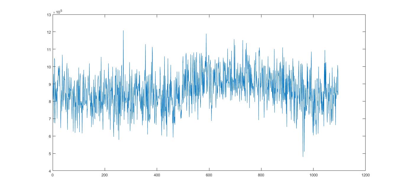
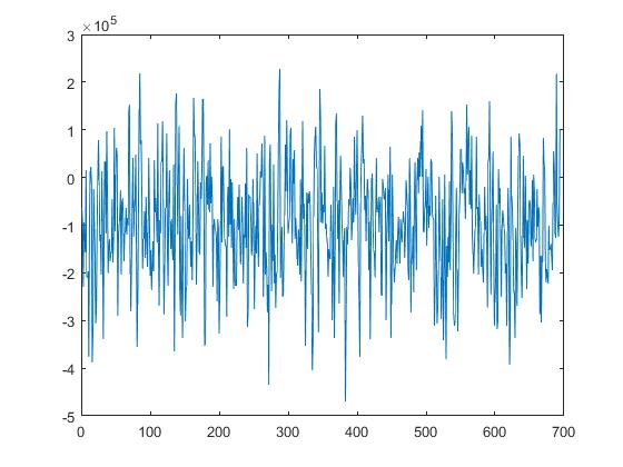
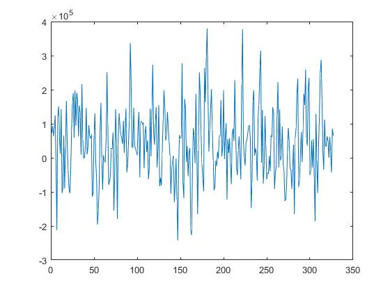
Hello, I have a problem with internal test wave signal. Here is my schematic and matlab plot. Is it possible that I have some issues in shematic?

These are the voltages of ADS1299 chip:

  1.  Vcap1 = -1.36V
  2. Vcap2 = -1.36V
  3. Vcap3 = 1.84V
  4. Vcap4 = 4.64 V

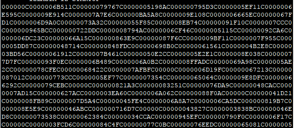
This is how register are configured : 

rc=write_byte(CONFIG1,"\96")
	 rc=write_byte(CONFIG2,"\D1")
	 rc=write_byte(CONFIG3,"\E0")
	 rc=write_byte(LOFF,"\00")
	 rc=write_byte(CH1SET,"\05")
	 rc=write_byte(CH2SET,"\01")
	 rc=write_byte(CH3SET,"\01")
	 rc=write_byte(CH4SET,"\01")
	 rc=write_byte(CH5SET,"\01")
	 rc=write_byte(CH6SET,"\01")
	 rc=write_byte(CH7SET,"\01")
	 rc=write_byte(CH8SET,"\01")


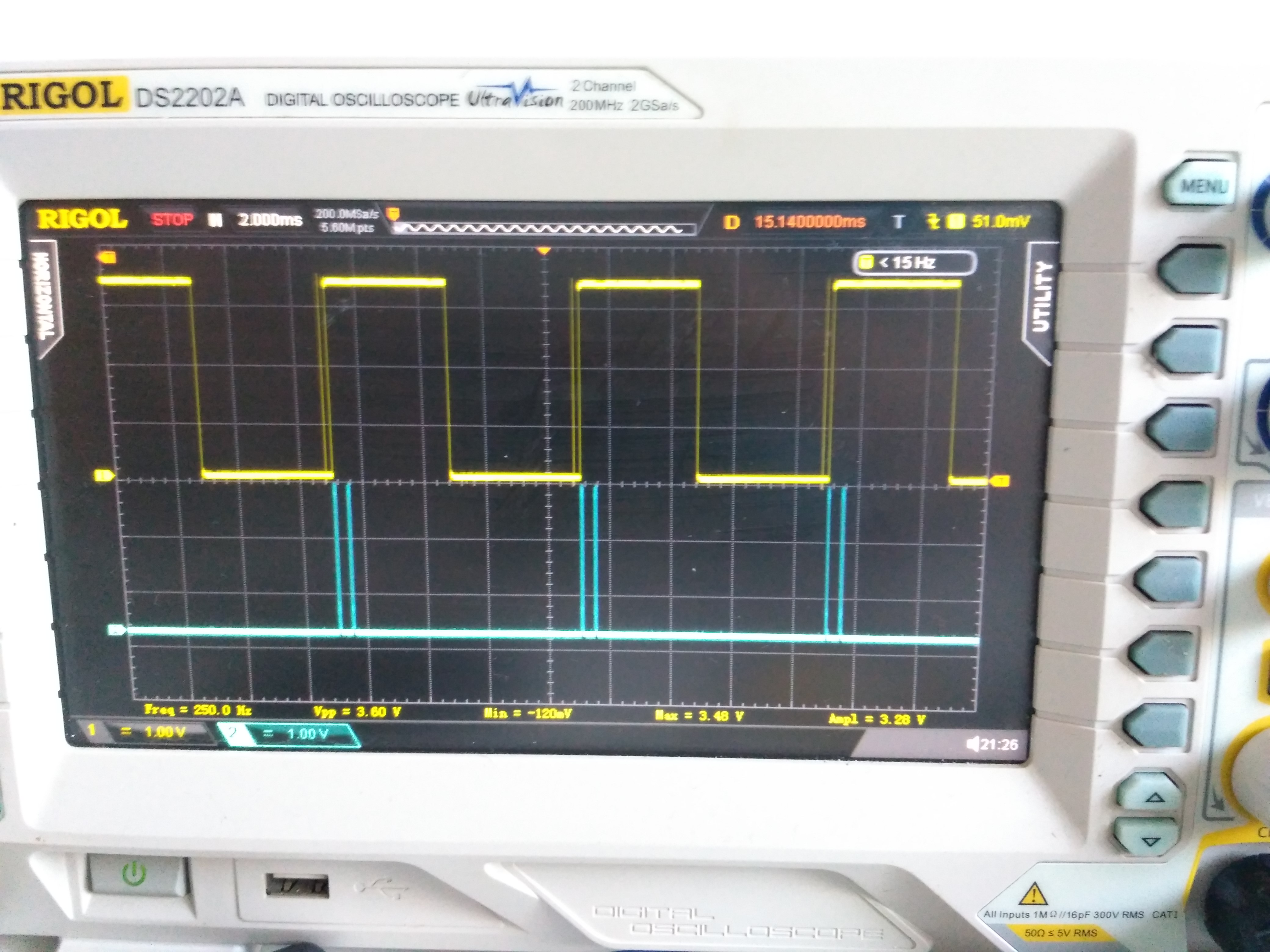
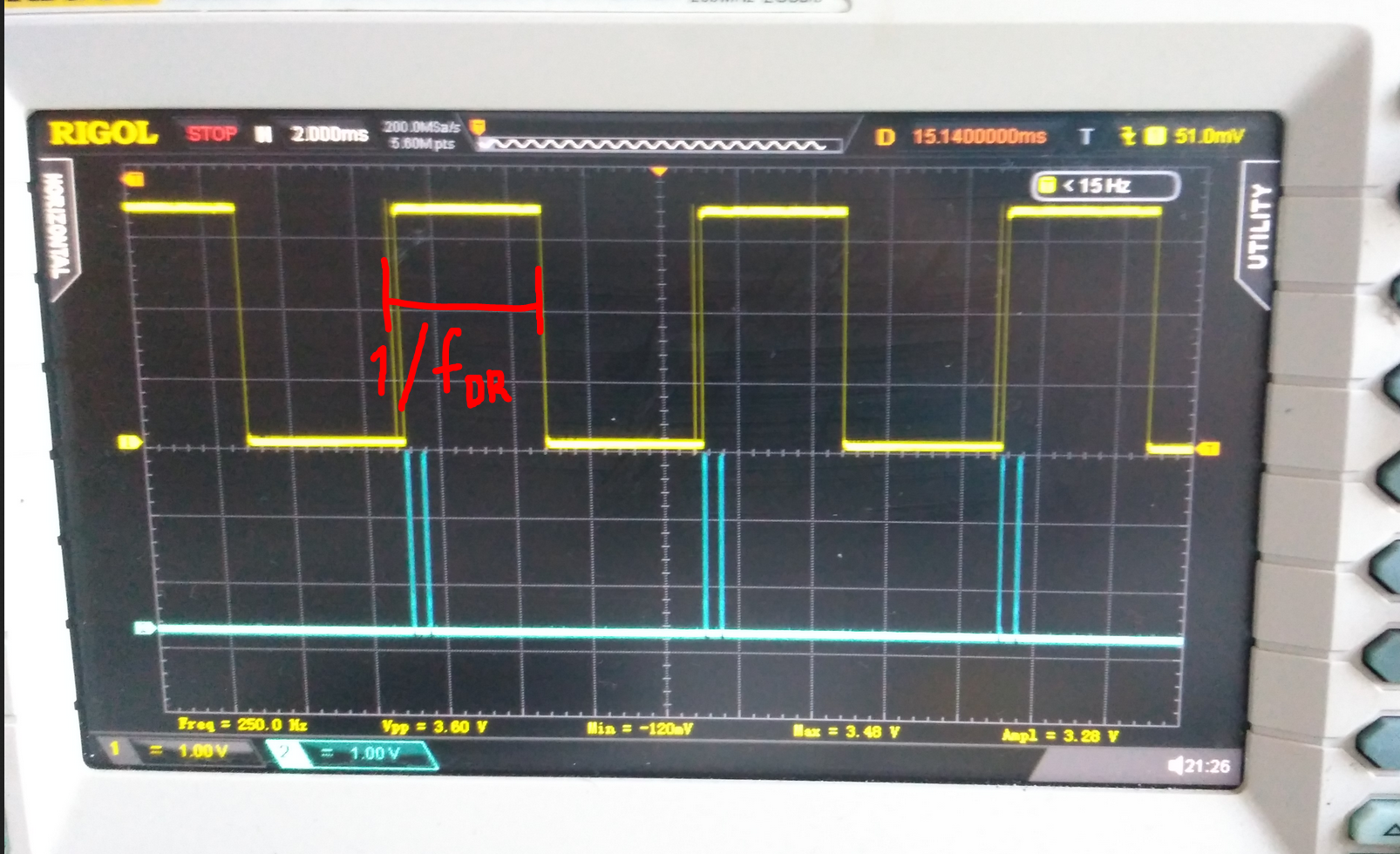
I'm clocking out data of only one channel over DRDY event. SPI clock is 250kHz.

  • Hello Mate,

    Thanks for your post.

    Your register settings look fine.

    It looks like you are clocking out the STATUS word and Channel 1 data. As long as you are in RDATAC mode, I don't believe reading only STATUS + CH1 would cause any issues.

    Could you share a capture from a logic analyzer? I glanced at the data you shared above and, in some cases, I can see the STATUS word repeating in the middle of your data acquisition. The STATUS word will always begin with the first byte as 0xC0, followed by the remaining 16 bits and then Channel 1 data. Using the logic analyzer, you may notice that /DRDY is pulsing low in the middle of the data acquisition.

    Make sure that you are monitoring for the falling edge of /DRDY. Your register settings have the ADS1299 configured for an output data rate of 250 SPS. You should have plenty of time to read only 48 bits.

    Best Regards,

  • Hi Ryan,

    Thank you for your reply. This picture is the scope from SCLK and DRDY pin. Second one is zoomed.

    Zoomed:

    I'm kindda lost here so if there is anything I can do to provide you with more information I'll be happy to do so.

    Regarding clocking out a status word, I'm aware what that means because I was working on ADS1292R chip that works perfectly with similar plot matlab code

    Can you observe VCAP1 voltage. I've read that it has to be above positive 1.1 Volts. Mine is negative ?

  • Hello Mate,

    From the first image, you can see that you are not reading every sample. You need to detect the falling edge of /DRDY, enable the interface, and clock out the data. In your images, /DRDY falls low and remains low for awhile. Then it returns high moments before the next /DRDY falling edge (similar to Figure 42). Also, you SCLK is approximately 500 kHz.

    Regarding VCAP1, are you using bipolar supplies (i.e. AVSS  = -2.5 V, AVDD = +2.5 V)? VCAP1 should measure AVSS + 1.2 V, so -1.3 V with respect to ground is acceptable.

    Best Regards,

  • This should be fine now. But results are the same. I'm reading data at 9200 baud rate and SCLK rate is 250kHz

    This is power up sequence and register setup :

    	GpioWrite(CS,0)
    	GpioWrite(PWD,0)//powerdown active low 
    	Delay(100)//ms
    	GpioWrite(PWD,1)//powerup
    	GpioWrite(RESET1,1)//reset tied high
    	Delay(50)//ms
    	rc=send_command("\11")//SDATAC
    	Delay(1)//ms
    	rc=send_command(RESET)//RESET
    	
    	rc=write_byte(CONFIG1,"\96")
    	rc=write_byte(CONFIG2,"\D0")//C0
    	rc=write_byte(CONFIG3,"\E0")
    	rc=write_byte(CH1SET,"\05")
    	rc=write_byte(CH2SET,"\E1")
    	rc=write_byte(CH3SET,"\E1")
    	rc=write_byte(CH4SET,"\E1")
    	rc=write_byte(CH5SET,"\E1")
    	rc=write_byte(CH6SET,"\E1")
    	rc=write_byte(CH7SET,"\E1")
    	rc=write_byte(CH8SET,"\E1")
    
    	rc=send_command(START)//START
    	rc=send_command(RDATAC) //send RDATAC- read data continuously


    For above code registers looks like this :

    And waveform is like this : 

    For diffferent configuration of CH1set:

    Waveform looks like this : 

    When I change from input short to test signal at CH1SET register, according to upper graphs, it seems like the signal is same for both configurations?

    If CH1SET register is set to h03 I get Full scale 7F FF FF.

    What could cause these kind of readings?