


Hi,
Let me ask you following questions about Vref/Vbias, Xin specifications.
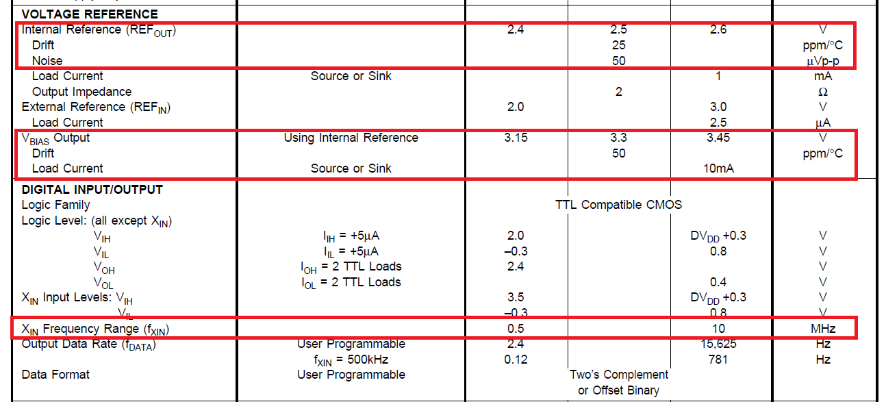
1) Vref
The Vref value of the specification is from 2.4V(min) to 2.6V(max), and the temperture specified is from -40 to +85℃.
My question is that the Vref value is fixed at one value of between 2.4V and 2.6V within -40 to +85℃, correct?
For example, once the value is 2.55V fixed at 25℃, the value is almost same as 2.55V with drift(25 ppm/℃) during the temperature. (not changed)
Or the value is possibly to cahnge to between 2.4V and 2.6V with temperature drift??
2) Vref drift
The specification is 25ppm/℃, but this is "typ" value.
Will you tell me the max value, if possible?
3) VBIAS
VBIAS is generated from Vref, I think.
So I suppose the "min-max" value range has almost same relation with Vref.
Why is the "drift" value 50ppm/℃ against the one of Vref, 25ppm? (2 times large)
4) Xin
Will you tell me the specification of Xin error/margin at 10MHz?
For example, the margin should be within +/-50ppm.
As I know this device is too old to check the specifications, I would be also glad even though your answer is just general infomation.
Thank you for your support in advance.
Best Regards,

