This thread has been locked.

If you have a related question, please click the "Ask a related question" button in the top right corner. The newly created question will be automatically linked to this question.

ADS4249EVM: Problem with the activation of digital functions (gain, offset correction, test patterns) of ADS4249 on ADS4249EVM

Part Number: ADS4249EVM
Other Parts Discussed in Thread: ADS4249

Hello,

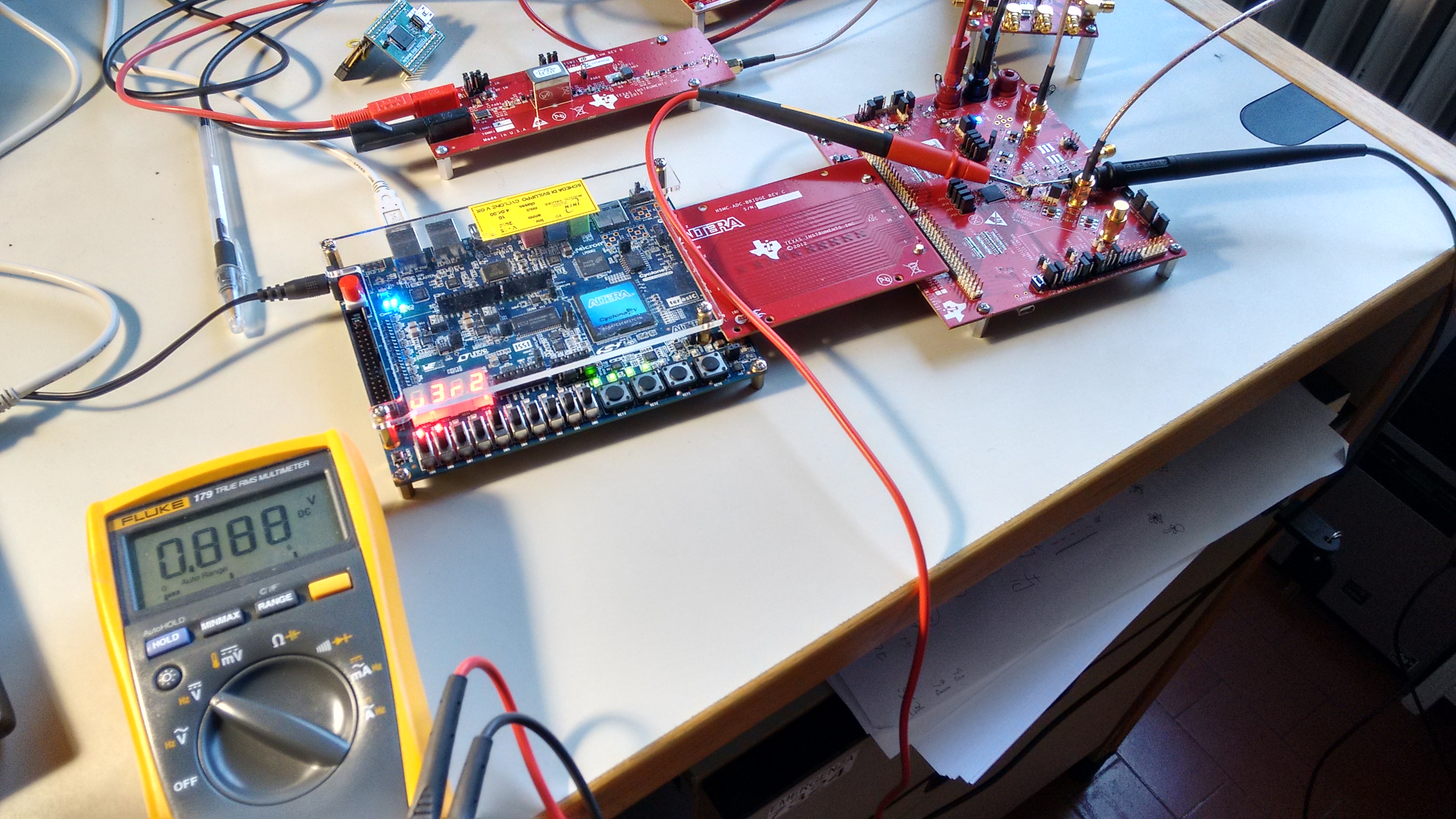
I am working with the ADS4249EVM board and I am able to correctly read the ADC digitized data (with a 245.7MHz clock and 10MHz input waveform) through an Altera Cyclone V FPGA (GX Starter Kit) and an HSMC/LVDS bridge.

The problem seems to be the serial communication with the ADC ADS4249, which is also managed by the FPGA (for this I have modified accordingly the board layout by moving the 0Ohm resistors R33, R30 and R47 to R68, R69, R70  and adding R128 ). The behavior I observe is the following:

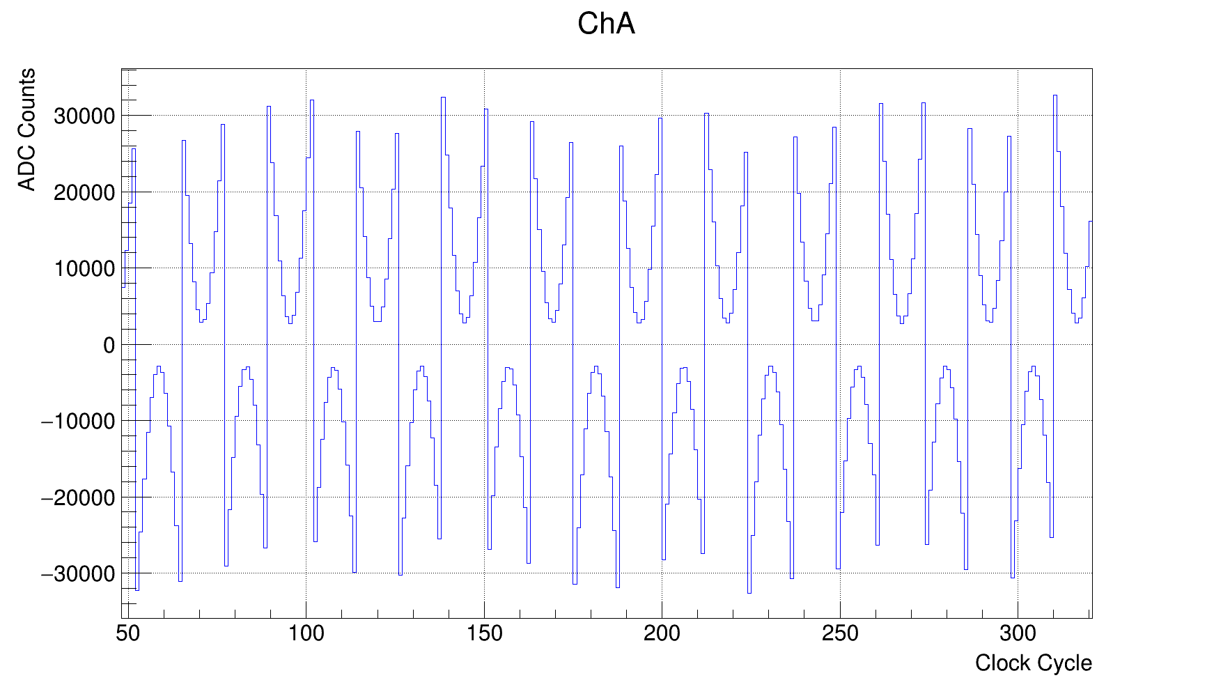
1) I can switch correctly from offset binary to two's complement representations (I see the results on the output data of the digitized 10MHz sine wave):

      Register 0x29, bits 4:3

2) I can correctly enable the HIGH PERF MODE of the ADC (I see that the VCM changes from 0.95 to 0.87 as pointed out in the datasheet):

      Register address = 2h, data = 40h
      Register address = D5h, data = 18h
      Register address = D7h, data = 0Ch
      Register address = DBh, data = 20h

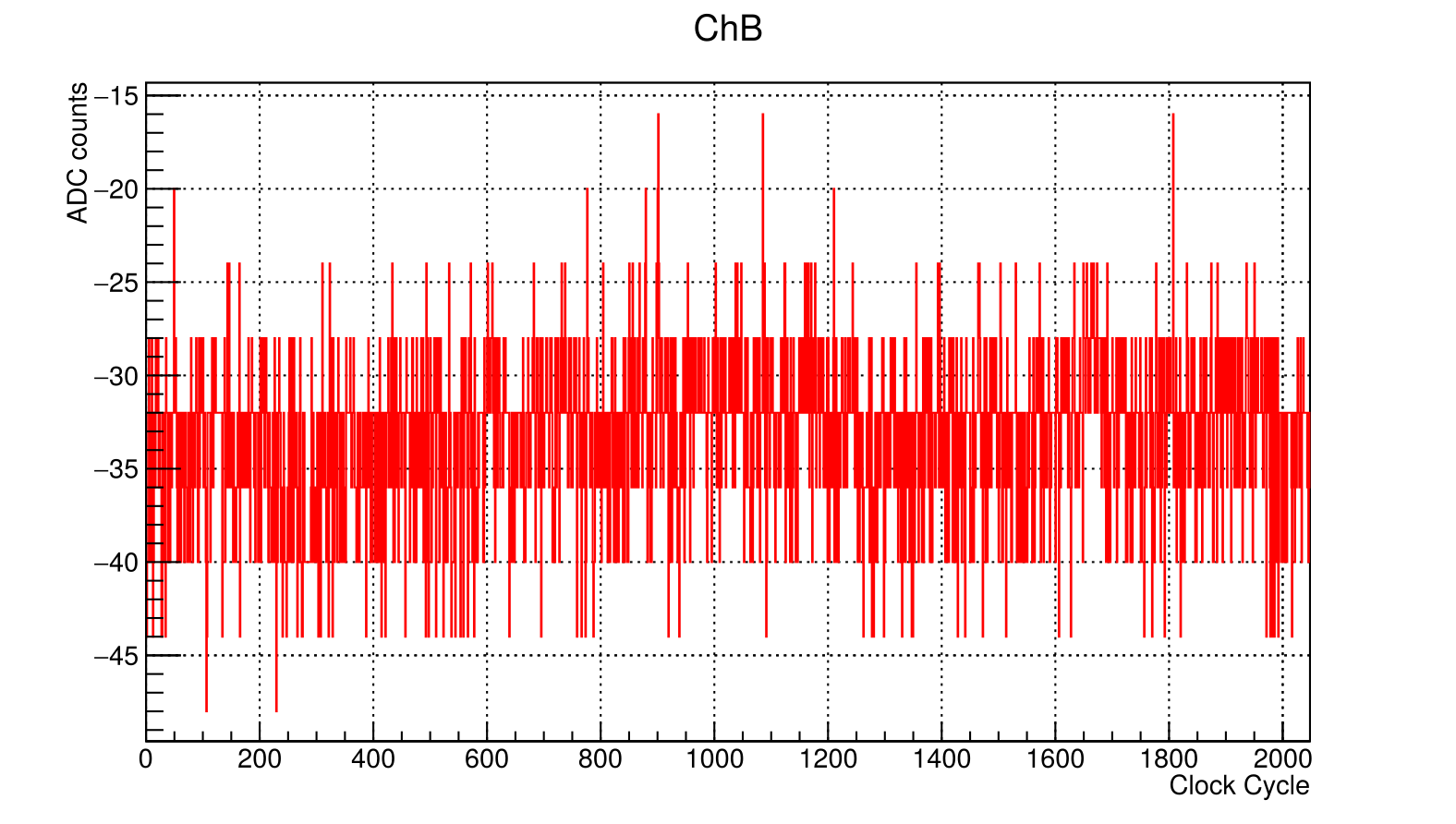
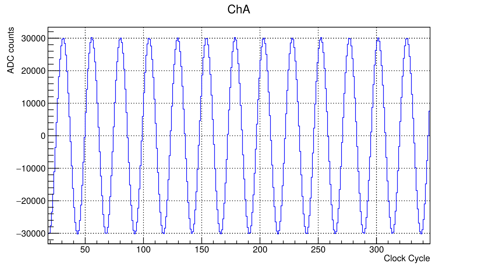
3) I cannot manage to change the output by enabling the EN DIGITAL bit (register 0x42, bit 3) and then activating a digital function (e.g. test patterns, gain ...). The ADC seems to ignore such settings even if the value seems to be written successfully to the register. The output I get is still the 10 MHz waveform (input channel A) and noise (channel B is not connected).


4) I can correctly read back whatever I write to the serial registers of the ADC, also in the registers which seems to have no effect.

The clock I am using for serial interface is 5 MHz, which should be fine according to the datasheet (max 20MHz). Also according to the datasheet, to activate a digital function, let's say a test pattern, it seems sufficient to set HIGH the EN DIGITAL bit and then chose the desired pattern mode, for example Register 0x25 with data 0x4 should give a RAMP on the LVDS output pins.

Since I would like to employ the digital functions in my work, my question is if there is something wrong on the ADC side (is the register map of the datasheet correct? is the serial interface with digital functions working for you?) or if I have got something wrong in my design.

Thank you in advance

  • Hi Michel,

    We are looking at your issue and will get back to you as soon as we can.

    Regards,
    Neeraj
  • Michelangelo,

    To get the test patterns to work, you have to enable the digital functions by writing a 0x08 to address 0x42.

    Regards,

    Jim

  • Hi Neeraj,
    thank you for the reply, I'll wait for the updates

    Regards,
    Michelangelo
  • Hi Jim,
    as described in point 3) of the thread this seems exactly to be the problem. I don't get any results when I write 0x8 to address 0x42 and then try to activate some digital function. Moreover what seems strange to me is that I am able to correctly read out the written value (0x8) by enabling the serial readout mode.

    Regards,
    Michelangelo
  • ADS4249 Registers:
    
    0x00 0x00
    0x01 0x00
    0x03 0x00
    0x25 0x04
    0x26 0x00
    0x28 0x00
    0x29 0x00
    0x2b 0x04
    0x2d 0x00
    0x2e 0x00
    0x3d 0x00
    0x3f 0x00
    0x40 0x00
    0x41 0x00
    0x42 0x08
    0x44 0x00
    0x45 0x00
    0x4a 0x00
    0x58 0x00
    0xbf 0x00
    0xc1 0x00
    0xcf 0x00
    0xd2 0x00
    0xd5 0x00
    0xd7 0x00
    0xd8 0x00
    0xdb 0x00
    0xea 0x00
    0xef 0x00
    0xf1 0x00
    0xf2 0x00


    Michelangelo,

    Attached are the register settings used to generate a ramp output on our EVM. See if these settings work for you. Also make sure to apply either an external reset or soft reset after power and clock is present before loading the registers.

    Regards,

    Jim

  • Hi Jim,

    thank you for the reply. Unfortunately I do confirm that such a register configuration does not work for me. I have tried with both hardware and software reset, then setting the registers as you described and checking the settings by enabling the read out mode and reading them back (as explained, I can successfully read back the registers with the correct values).

    It all seems in place, still my output on both channels does not change from the default one (10MHz waveform on ch-a and ch-b not connected):

    Despite the fact that I am able to read back what I have written, I can also correctly change the channel outputs from two's complement to offset binary representation. Moreover I am also able to enable the HIGH PERF MODE (an achievement which seems to confirm the good behavior of my serial interface), as I show in the following figure (the VCM goes from 0.95 to 0.88 as described in the ADS4249 datasheet for HIGH PERF MODE):

    For these reasons I was wondering if you have tested the serial communication with ADS4249EVM, in order to understand whether there is some error/wrong register map for the ADS4249 or if there is still some bug on my serial interface (even if it seems to work correctly, as explained in my initial post and in the previous image).

    Regards,

    Michelangelo

  • Michelangelo,

    You need to enable digital (disable low-latency) mode (i.e. set reg 0x42 bit 3) before programming the test patterns.

    Regards,

    Jim

  • Hi Jim,

    thank you for the suggestion, unfortunately the situation remains the very same described in my previous reply.

    Is the ADS4249 serial interface working for you?

    Regards,

    Michelangelo

    P.S.

    Here is reported the correct activation of the offset binary numeric representation (through the register 0x29, data 0x18).

    The numbers are represented in offset binary while they are read back in two's complement notation. Hence the waveform appears

    distorted. If I switch back to two's complement notation the following waveform comes back to its correct form, as attached in my

    previous reply. Everything seems to work as expected here.

  • Hi Michelangelo,

    After powering up the device, you must first clear the contents of all SPI registers either through RESET pin or through register bit (0x0, 0x2).

    Assuming you are already applying the reset:
    1. Are you able to directly program the test patterns (0x25 0x04; 0x2b 0x04) after you reset the device - without selecting EN DIGITAL bit (reg 0x42, bit 3)?
    2. Can you reset the device(0x0, 0x2), put device in read-back mode(0x0,0x1), read contents of register 0x42. What do you get?

    Regards,
    Sourabh
  • Hi Sourabh,

    thank you for the the reply. Yes, as you said I am issuing a reset after the device power up.

    Answering to your questions:
    1. Yes I am able to write on the test patterns registers after the reset of the device and without the EN DIGITAL bit activated. I can correctly write and read back what I have written (e.g. 0x25 0x4; 0x2b 0x4), but still nothing happens to the ADC output. I still see the digitized analog input signals that I am applying.
    2. After a reset, if I read out the 0x42 register I get the 0x00 value.

    Regards,
    Michelangelo
  • Michelangelo,

    It appears you may have a defective board. Did you order this through a distributor? If so, can you work with them on getting a replacement board?

    Regards,

    Jim 

  • Michelangelo,

    Are you still having issues with this board? If so, we may look into getting you a replacement one. Let us know.

    Regards,

    Jim

  • Hi Jim,

    sorry for the delay in the answer, I have been quite busy on other projects lately.
    Yes, the board does still have the same issues and I would be happy to replace it.
    I ordered it through an Italian distributor, so I think I should first ask them for a replacement,
    and then I'll let you know what happens.

    Thank you,
    Michelangelo
  • Michelangelo,

    if your issues still persist there is a chance that your device is actually faulty and in that case we would recommend you return it to TI for further analysis. Please le us know if you want to go down that route.

    Matthiass