Other Parts Discussed in Thread: ADS1274
Hi,
I am looking to design a device which requires having ADS1174 converters daisy-chained, synchronized samples, over two PCBs using a cable to connect them together (one ADC on each PCB). Do you have any documentation about a similar use case?
I want to understand and evaluate what are the limitations of such a design, especially regarding the timings and possible delays between signals (clocks and data).
In the datasheet, I have found information about delays and how data are chained from one device to the next.
"The phase match of one four-channel ADS1174 to that of another ADS1174 may not have the same degree of sampling match (the same is true for two 8-channel ADS1178s). As a result of manufacturing variations, differences in internal propagation delay of the internal CLK signal coupled with differences of the arrival of the external CLK signal to each device may cause larger sampling match errors. Equal length CLK traces or external clock distribution devices can be used to control the arrival of the CLK signals to help reduce the sampling match error."
This quoe is from the subsection "sampling aperture matching" in page 10. Here, "sampling match errors" refers to output samples from one ADC being out of phase with output sample of another ADC in the same chain due to delays on the CLK signal? I did not found a value to quantify this matching error. Does it depend on the CLK frequency (lowering the frequency can increase the degree of sampling match if CLK signals are slightly out of sync) ?
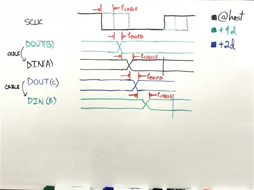
"Since DOUT1 and DIN are both shifted on the falling edge of SCLK, the propagation delay on DOUT1 creates a setup time for DIN. Minimize the skew in SCLK to avoid timing violations."
The propagation delay, in this case, is the time from the DOUT1 of the first ADS to the DIN of the second one?
Additionally, I read that in frame-sync serial mode "The MSB data become valid on DOUT on the SCLK rising edge prior to FSYNC going high". Does this mean that the MSB bit is only present on DOUT1 for half an SCLK period since the subsequent bit should be shifted out on the next falling edge?
By any chance would you have a graph/chronogram that explains how data is propagated from one ADC to the next one?
Thank you very much.
Best regards


