Hi,
Currently I'm experiencing some trouble getting the ADS4129 ADC to source any of the in built test patterns. For instance, I programmed the data 0x02 to the register with address 0x25 first, in order to get the ADC to output an all 1's pattern as mentioned in the datasheet. But the output bits still appear to toggle as in normal operation, instead of staying all 1's.
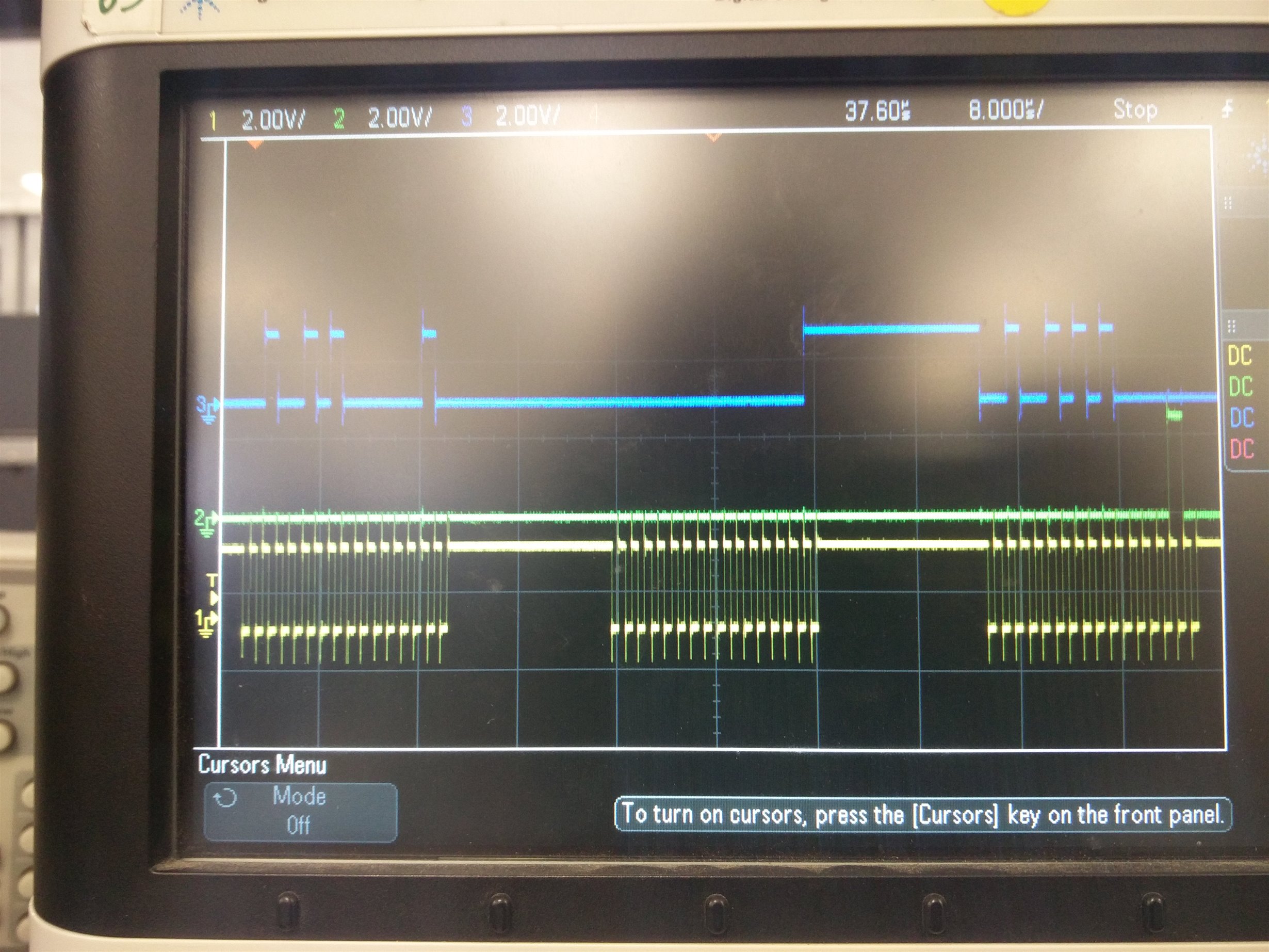
To rule out any SPI programming timing related issue etc, I did a readback via the OVR-SDOUT pin as well, and the read back data from 0x25 addressed reg appears to match the written data, ie, 0x02. Please find attached snapshots of the sequence I followed where:
- I first programmed the data 0x02 to the register with address 0x25
- Then programmed the data 0x02 to the register with address 0x00 to enable SDOUT readback,
- And finally programmed the dummy data 0x05 to the register with address 0x25 again for reading it back, in which case I seem to observe the expected value on SDOUT.
In the attached plot, blue trace is the SDIN, Yellow trace the SCLK signal and Green the SDOUT signal.
I suppose SDOUT matching the written value means programming is correct? Can you please comment on what may be going wrong here? I needed to get the test pattern sourcing to get started with the work on fixing my FPGA capture timing
Thanks,
Anoop


