This thread has been locked.

If you have a related question, please click the "Ask a related question" button in the top right corner. The newly created question will be automatically linked to this question.

ADS1274: Channel failures of ADS1274 - what is the failure mechanism?

Part Number: ADS1274
Other Parts Discussed in Thread: ADS1278

We have been using the ADS1274 in our product since 2011 and built over 1000 of these devices without ADC failure issues.  We first encountered an ADC failure in Feb 2016 and more recently have experienced a dozen or more ADC channel failures with recently fielded products.  Most of these have been at a specific site and we are struggling to understand what environmental stresses at this particular site are causing the failure.

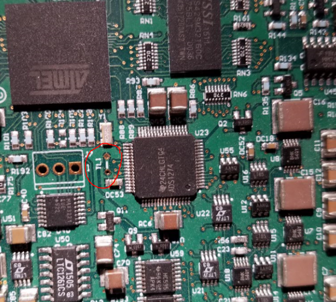
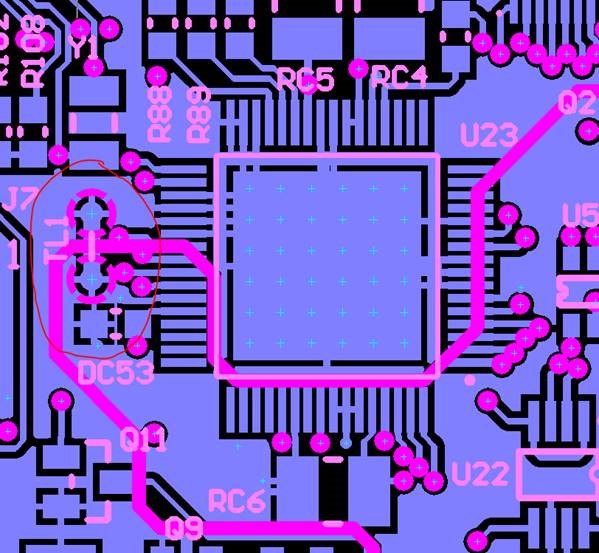
I have read Ryan's description of how a greater than 300 mv differential between the analog and digital grounds could be a source of the failures.  Our board layout nearly exactly copied the application note layout guidelines and has the tie point between the analog and digital grounds adjacent to the ADC.  That's TL1 in the photo below. We have not changed this part of the layout since 2011.

I am looking for some guidance on what the failure mechanism is and what environmental stresses are likely to induce the failures.  We certainly have been looking at things like dirty mains power, EMF, and ESD at this site but none of those phenomena appear to be any different than the dozens of other industrial sites where our product does its job every day without failure.

I can certainly provide a ton more details about what we have done and what we know about the failures but perhaps someone has some thoughts to share that can steer the conversation and our investigation in a useful direction.

Thanks,

Dana

  • Hi Dana,

    Welcome to our e2e Forum! Can you describe the ADS1274 failure a little more? Does the issue happen with a single channel - i.e. one channel has bad data but the others are fine, or is is a gross failure of the whole device? Does removing and replacing a bad device bring the unit back to operational state (i.e. no additional components damaged, only the ADC)? Your picture did not come through with your post, so we don't see 'TL1' - if you can try posting that again, we'd appreciate it!

  • The ADC Channel failures are a positive rail lock up where the digital output is stuck at 0x007F FFFF.  This usually happens on Channel 1 but we have had two cases where this has happened on Channel 2.  In all cases the other 3 three channels work normally after the single channel failure.  We have replaced a number of these failed ADCs and every replacement restored full functionally to the device so it does not appear that any other components or the PCB itself were damaged, just the TI ADC.  We also have very carefully inspected and tested all the solder pin connections on failed units to determine if there were assembly defects that could be causing the failure.  All the failed boards have passed these tests without any indication of an assembly defect.

    BTW, the 'Ryan' I referred to above is TI's Ryan Andrews who seems to participate in this blog frequently.

    The failure mode is along the lines of these other threads from this TI community blog:

    I have attempted to attach the photo of the ADC on the PCB again as part of this response.

    I can provide even more details if it helps you get to a point where you can share possible environmental stresses that can lead to this type of component failure.  My goal is to get some guidance on where to take the investigation from here.  We are expending a lot resources trying to track this down but few clues exist as to root cause so targeting a specific type of environmental stress would be helpful.

    Thanks,

    Dana

  • Hi Dana!

    Thank you for the additional detail! I know Ryan pretty well - he actually sits about 6 feet away from me. With a single channel failure, we'd normally start looking at the differences in the routing between the problematic channel and the ones that don't show any issues. Of course, this also carries the assumption that the input signals to all channels are essentially equal.

    If it is OK with you, I'll send you a note to your my.TI profile e-mail address in an effort to get an internal failure analysis started. It would be interesting to take a look at some of the failed units you have. From there, hopefully you can share more of your schematic and layout with us so that we can try to pinpoint what the issue might be.
  • Direct contact sounds like a great plan. This is a very important issue for us and I appreciate your rapid response.

    Dana
  • This is a follow up post to tell the story of what has happened since I started this thread last November.

    Tom Hendricks from TI did indeed contact me directly and we had several email exchanges and he had a conference call or two with our design team.

    Also since last posting to this forum we have spent a considerable amount of time performing ESD and EFT (Electrical Fast Transient) testing on samples attempting to replicate the failure mode the device was suffering in the field.  Eventually we hit on a particular EFT pattern that would predictably kill channels of the ADC. This pattern was coupled into the device via the USB charging port.

    We attacked the ADC failure issue in several ways:

    1. We decided to move to the ADS1278 8 channel 'high reliability version' that is essentially the same design but with the additional 4 channels active and a broader temperature rating.  We decided to avoid using channels 1 and 2 of the device as these are the channels that suffered the lock up failures with the ADS1274. We prototyped this device onto our existing PCB layout by lifting pins and jumping from pad to pin.  Messy but effective.  We exposed four ADS1278 prototype boards to the EFT test.  We had mixed results.  Two survived this test but two suffered what appears to be in an internal shorting of the 3.3 volt power supply. This did not give us great confidence that simply moving to the 8 channel device and avoiding channels 1 and 2 was going to be effective at preventing failures.

    2. After talking with Tom again he nudged us to reevaluate the way the analog and digital ground planes are tied together. He suggested we eliminate the track link (mentioned above) and use the PowerPad under the ADC as the only link between the analog and digital sides of the ground plane.  After a bit of back and forth with the layout people we pressed forward with a board spin that implemented this change. Tom made the time to review our design changes and provided guidance on how best to implement the changes. Due to some issues outside of our control it took many weeks to get a pilot run of 9 boards built that we could use for testing. These were delivered to us a couple of weeks ago and we tested them using the same EFT generator and signal pattern that we found would predictably kill our current production boards’ ADC.

    Here are some images that show how the PCB layout was changed:

    Looking up from the bottom, the top layer with overlay of GND Plane and drill pattern for vias.

    (GND plane is reverse image such that pinkish color represents areas with NO copper)

    Screen grabs are intended to show how the vias (yellow ‘+’) link the top, bottom, and ground planes together.

    The two parts of GND Layer for Analog and Digital ground regions are indeed only linked together by the PowerPad region on the top layer.


    This image is from the current production design.  A view from the top showing this same region around the ADC and I circled in red the TL1 ‘track link’ where the analog and digital sections of the ground planes are linked.  Based on conventional design practice this track link is located in very close proximity to the ADC.

    *****

    The great news is the changes resulted in a device that is immune to even the worst 5 KV EFT pulses we could generate with the test instrument. Several of the samples were subjected to over 45 minutes of various EFT patterns and amplitudes with no failures of the ADC. One of the boards had a failure in another unrelated area of the device but we attribute that to abuse we gave it using the EFT generator.

    Thanks goes to Tom Hendricks for his design help and his persistence in convincing us to take on the evaluation and redesign of the ground plane linking. We think this was the key change that appears to have solved the issue. Moving to the ADS1278 was simply added insurance.

    Next we have four of these pilot run boards heading to a field trial. Having this design survive for several months at the industrial site that has routinely been destroying ADCs will make me a true believer that we have put this problem behind us.

    Dana