This thread has been locked.

If you have a related question, please click the "Ask a related question" button in the top right corner. The newly created question will be automatically linked to this question.

ADS1263: ADS1263IPW need help

Part Number: ADS1263
Other Parts Discussed in Thread: ADS1256, ADS1262

Hi

My customer need help with ADS1263IPW.

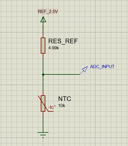
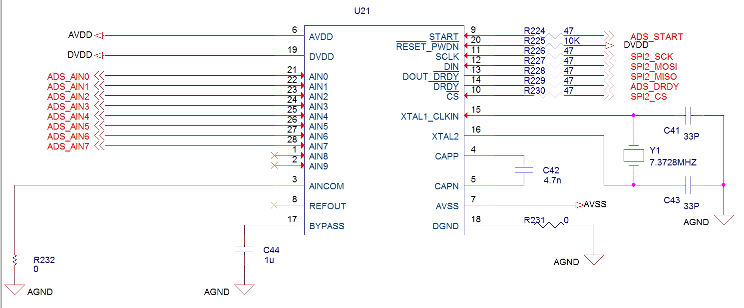
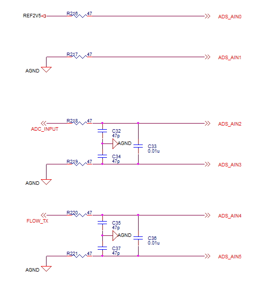
 When the external reference voltage is 2.5V (AIN0  ,AIN1 -), the second channel (AIN2)of ADC1 cannot be sampled, and the second channel(AIN2) of ADC2 is normal.Other channel sampling is normal. Why?
Register configuration is as follows:
void  write_ADS126xREG(void)       //单个写ADS1256寄存器
{  ADS126xSendStopCommand();
ADS126xSendADC2StopCommand();
ADS126xSendResetCommand();    //复位、校准
Reg_data[0]=0x03;
ADS126xWriteRegister(0x01,1,Reg_data);   //power REG ref,vbias,reset
Reg_data[0]=0x05;
ADS126xWriteRegister(0x02,1,Reg_data);   //Interface REG  status, CRC checksum  disable,  4data/6data
Reg_data[0]=0x00;
ADS126xWriteRegister(0x03,1,Reg_data);   //Mode0 REG runmode , chop , delay
Reg_data[0]=0x89;   //
ADS126xWriteRegister(0x05,1,Reg_data);   //Mode2 REG PGA Bypass Mode

Thanks

Star

  • Hi Poster!

    Our support staff are enjoying the Thanksgiving Holiday break with their family and friends. Please accept our apologies in advance for the delay this may cause in resolving your query. We expect normal support activity to resume on Monday, November 27th.
  • Hi Star,

    What is meant by "ADC1 cannot be sampled"? Are you getting invalid conversion results? If so, what are these results (0, full-scale, random, etc..)?

    I would double check the REFMUX and ADC2CFG register settings to make sure you are selecting the external reference on AIN0/1. However, for troubleshooting I would also recommend trying to use the internal reference, to see if that is providing similar or different results. That would give us more information as you what might be happening...

    Also,
    How is the input multiplexer configured (which two channels are you trying to sample)?
    And what are the input voltages provided to those channels?

    Thanks and best regards,
    Chris
  • hi,Chris,
    First, thank you for your answer.

    1.   Yes, the(ADC1) AIN2 channel sampling value is always full-scale when external reference input is 2.5 V.

    2.   When using internal reference voltage, (ADC1)AIN2 channel sampling is normal.

    3.  The (ADC1)AIN2 input voltage range is 0~2.5V.

    4.  The initialization configuration is as follows:

    void  Initialization_ADS126xREG(void)       //单个写ADS1256寄存器
    {      
     
       ADS126xSendStopCommand();
       ADS126xSendADC2StopCommand();
       delay_us(100);  
       ADS126xSendResetCommand();    //复位、校准
        
        Reg_data[0]=0x03;//使能内部参考,取消内部电平输出
        //Reg_data[0]=0x02;  //取消内部参考
        ADS126xWriteRegister(0x01,1,Reg_data);   //power REG ref,vbias,reset
      
       Reg_data[0]=0x05;
        ADS126xWriteRegister(0x02,1,Reg_data);   //Interface REG    status,  CRC checksum  disable,  4data/6data
      
       Reg_data[0]=0x00;
        ADS126xWriteRegister(0x03,1,Reg_data);   //Mode0 REG runmode , chop , delay
      
       Reg_data[0]=0x80;   //取消电流源
      //Reg_data[0]=0x96;  //10M电阻
       ADS126xWriteRegister(0x04,1,Reg_data);   //Mode1 REG Bias ADC Connection,Sensor Bias Polarity,sensor bias current
      

        Reg_data[0]=0x89;   //DISable PGA  Data Rate 1200sps
        ADS126xWriteRegister(0x05,1,Reg_data);   //Mode2 REG PGA Bypass Mode,  Gain, Data Rate 1200sps
      
       //Reg_data[0]=0x01; // AIN0+, AIN1-
         Reg_data[0]=0x23; // AIN2+, AIN3-   //TEMP
        // Reg_data[0]=0x21; // AIN2+, AINCOM-   //TEMP
       //Reg_data[0]=0x45; // AIN4+, AIN5-   //FLOW
       //Reg_data[0]=0x67; // AIN6+, AIN7-   //PMT   
       //Reg_data[0]=0xee;   //TDACP  TDACN  选择输入端
       //Reg_data[0]=0xbb; //测温
          ADS126xWriteRegister(0x06,1,Reg_data);   //Input Multiplexer REG Positive Input, Negative Input Multiplexer AIN0+, AIN1-


       Reg_data[0]=0xbb;  //不连接
        ADS126xWriteRegister(0x0d,1,Reg_data);   //IDAC Multiplexer REG IDAC2,IDAC1 Output Multiplexer  No Connection

         Reg_data[0]=0x00;  //OFF
         ADS126xWriteRegister(0x0e,1,Reg_data);   //IDAC Multiplexer REG Selects the current values of IDAC1 /IDAC2  OFF
       
       //Reg_data[0]=0x00;  //内部参考2.5V
       Reg_data[0]=0x11;  //外部参考2.5V
        ADS126xWriteRegister(0x0f,1,Reg_data);   //Reference Multiplexer REG Reference Positive/Negative Input 内部2.5V
       

       Reg_data[0]=0x13; //page54  positive  2.4688v
        ADS126xWriteRegister(0x10,1,Reg_data);   //TDAC  DACP=1.5V    page54


       Reg_data[0]=0x14; //page54  negative  2.4375v  
        ADS126xWriteRegister(0x11,1,Reg_data);   //TDAC   DACN=0.5V   page54
       
       //ADC2

       Reg_data[0]=0x48;   //1V/V  bypass  external 2.5V
       ADS126xWriteRegister(0x15,1,Reg_data);   //ADC2 Configuration REG ADC2 Data Rate /Reference Input /Gain   100SPS  2.5V  1V/V
       
       //ADC2
       //Reg_data[0]=0x23;  //AIN2+, AIN3-
       Reg_data[0]=0xbb;  //测温
        ADS126xWriteRegister(0x16,1,Reg_data);   //ADC2 Input Multiplexer REG Selects the ADC2 positive/Negative  input  AIN2+, AIN3-

       ADS126xSendStartCommand(); 
       ADS126xSendADC2StartCommand();
     
    }

    Thanks and best regards,

    Star

    My phone number: +86  189-168-356-25

  • Hi Star,

    Thanks for the additional details.

    user4733497 said:

    1.   Yes, the(ADC1) AIN2 channel sampling value is always full-scale when external reference input is 2.5 V.

    2.   When using internal reference voltage, (ADC1)AIN2 channel sampling is normal.

    This would make it seem like there might be an issue with the external reference voltage...

    user4733497 said:
       Reg_data[0]=0x11;  //外部参考2.5V
        ADS126xWriteRegister(0x0f,1,Reg_data);   //Reference Multiplexer REG Reference Positive/Negative Input 内部2.5V

    This might be the problem... Programming the REFMUX register to "0x11" selects AIN2/AIN1 pins as the external reference source. This should be changed to "0x09" to select the AIN0/AIN1 pins.

    For the ADC2CFG register, use "0x08" to select AIN0/AIN1 for the reference source to ADC2.

    Try the above change and let me know if that resolves your issue!

    If you still have problems after making that change, then I would ask/suggest the following...

    • What is your external reference source, and would you be able to share a schematic of it?
    • You might want to try measuring the AIN0/1 voltage using the internal reference to check what voltage the ADC is seeing on these pins.

    Thanks and best regards,
    Chris

  • Chris,

    Thank you very much. AIN2 sampling exception problem solved.


    Also, excuse me:

    When using internal 2.5V reference voltage, why is the sampling value inaccurate?

    For example, the input voltage is 1.2676V and the sample value is 1.8387V,1.8452V,1.8101V,1.8605V,1.7608V,1.8028V,1.7851V,

    1.8753V,1.7727V......

    When the external reference 2.5V was used, the sampling voltage was 1.2676V when the input voltage was 1.2676V.
  • Hi,

    That is a large error and an unreasonable about of noise, very uncharacteristic of the ADS1262... I calculated a ~43% gain error and effective resolution of about 7-bits, which is way outside of the ADC specifications.

    Are you sure the registers were configured correctly when you collected this data?
    I would try resetting the device (since the internal reference is selected by default) and try programming the input multiplexer to select your input signal source.

    What are you using as your input signal source? And is this voltage ratiometric to your external reference source?
    In your previous register settings you had bypassed the ADS1262's internal PGA. Therefore, make sure your input source has a low-output impedance so that it can drive the delta-sigma modulator directly (otherwise, try enabling the PGA in a gain of 1 V/V). Also, if your input signal and external reference source are ratiometric, you might have a ratiometric error on both the input and reference voltage which is cancelled by the ratiometric measurement.

    Additionally, would you be able to share a schematic of your circuit?


    Thanks and best regards,
    Chris

  • Chris,

    1.Configuration is as follows:

    void  write_ADS126xREG(void)      
    {      
       ADS126xSendStopCommand();
       ADS126xSendADC2StopCommand();
       ADS126xSendResetCommand();    //复位、校准
        
        Reg_data[0]=0x03;//使能内部参考,取消内部电平输出
        ADS126xWriteRegister(0x01,1,Reg_data);   //power REG ref,vbias,reset
      
       Reg_data[0]=0x05;
        ADS126xWriteRegister(0x02,1,Reg_data);   //Interface REG    status,  CRC checksum  disable,  4data/6data
      
       Reg_data[0]=0x00;
        ADS126xWriteRegister(0x03,1,Reg_data);   //Mode0 REG runmode , chop , delay
      
       Reg_data[0]=0x80;   //取消电流源
        ADS126xWriteRegister(0x04,1,Reg_data);   //Mode1 REG Bias ADC Connection,Sensor Bias Polarity,sensor bias current
      
    //   Reg_data[0]=0x09; //enable PGA  1v/v
    //   Reg_data[0]=0x19; //enable PGA  2v/v
    //   Reg_data[0]=0x29; //enable PGA  4v/v
    //   Reg_data[0]=0x39; //enable PGA  8v/v
    //   Reg_data[0]=0x49; //enable PGA  16v/v
    //   Reg_data[0]=0x59; //enable PGA  32v/v

       Reg_data[0]=0x89;   //DISable PGA  Data Rate 1200sps
       ADS126xWriteRegister(0x05,1,Reg_data);   //Mode2 REG PGA Bypass Mode,  Gain, Data Rate 1200sps
      
       //Reg_data[0]=0x01; // AIN0+, AIN1-
         Reg_data[0]=0x23; // AIN2+, AIN3-   //TEMP

          ADS126xWriteRegister(0x06,1,Reg_data);   //Input Multiplexer REG Positive Input, Negative Input Multiplexer AIN0+, AIN1-
       
       Reg_data[0]=0xbb;  //不连接
        ADS126xWriteRegister(0x0d,1,Reg_data);   //IDAC Multiplexer REG IDAC2,IDAC1 Output Multiplexer  No Connection

         Reg_data[0]=0x00;  //OFF
          ADS126xWriteRegister(0x0e,1,Reg_data);   //IDAC Multiplexer REG Selects the current values of IDAC1 /IDAC2  OFF
       
       Reg_data[0]=0x00;  //内部参考2.5V  
       //Reg_data[0]=0x09;  //外部参考2.5V
       
        ADS126xWriteRegister(0x0f,1,Reg_data);   //Reference Multiplexer REG Reference Positive/Negative Input 内部2.5V
       

       Reg_data[0]=0x13; //page54  positive  2.4688v
       ADS126xWriteRegister(0x10,1,Reg_data);   //TDAC  DACP=1.5V    page54


       Reg_data[0]=0x14; //page54  negative  2.4375v
        ADS126xWriteRegister(0x11,1,Reg_data);   //TDAC   DACN=0.5V   page54
       
       //ADC2
      
       Reg_data[0]=0x48;   //1V/V  bypass  external 2.5V
       ADS126xWriteRegister(0x15,1,Reg_data);   //ADC2 Configuration REG ADC2 Data Rate /Reference Input /Gain   100SPS  2.5V  1V/V
       
       //ADC2
       //Reg_data[0]=0x23;  //AIN2+, AIN3-
       Reg_data[0]=0xbb;  //测温
        ADS126xWriteRegister(0x16,1,Reg_data);   //ADC2 Input Multiplexer REG Selects the ADC2 positive/Negative  input  AIN2+, AIN3-

       ADS126xSendStartCommand();
       
         ADS126xSendADC2StartCommand();
     
    }

     2.input signal source


    3. this voltage is ratiometric to external reference source.

    Other configurations are the same,Only change the reference voltage:

      //Reg_data[0]=0x00;  //内部参考2.5V  
       Reg_data[0]=0x09;  //外部参考2.5V
        ADS126xWriteRegister(0x0f,1,Reg_data);   //Reference Multiplexer REG Reference 


    4. schematic :  AVDD= 2.5V, AVSS= -2.5V, DVDD= 3.3V; REF2V5= 2.5V;


    5. Looking forward to your reply.


  • Hi,

    From looking at the schematic I noticed that the capacitor on the REFOUT pin is missing... The ADS1262 datasheet suggests the use of a 1uF cap on this pin. Without a capacitor on REFOUT it is possible for the internal reference to oscillate and cause the gain error you are seeing.

    Since your input signal is not coming for a low-output impedance source, but from a resistor divider, I would also highly recommend using the PGA (enabling it) to avoid additional gain errors as a result of the lower input impedance of the delta-sigma modulator when the PGA is bypassed.

    I would try adding a capacitor to the REFOUT pin to check if this resolves your issues with the internal reference; however, you probably want to stick with the external reference when measuring the NTC thermistor as it will provide a more ratiometric measurement.

    Best regards,
    Chris
  • Chris,

      Plus the capacitance problem solved.

      Thank you very much for your reply.

  • You're welcome! If you would, please click the "This Resolved My Issue" button on the solution.

    Let me know if you have any additional questions I can help with!

    Best regards,
    Chris