This thread has been locked.

If you have a related question, please click the "Ask a related question" button in the top right corner. The newly created question will be automatically linked to this question.

DAC161S997: PCB designed cannot use

Part Number: DAC161S997

Hi team,

A customer has problems about his PCB, the details are as follows, could you please help? Thank you!

DAC161S997 is used to design a 4-20mA driving circuit. The PCB is designed according to the schematic of DAC161S997EVM. All the chips are same except the power supply chip. Here arehe problem:

1. When powered up, the current is 80mA; the base voltage of triode3904 is 2.7V, what may cause it?

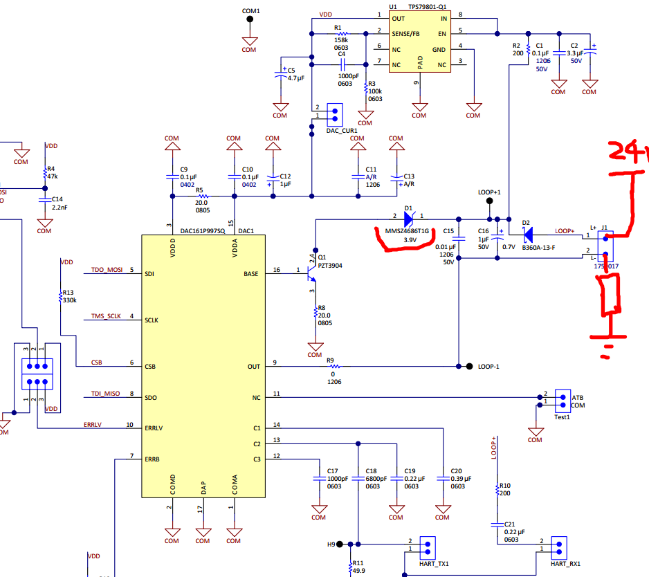
2. The output of LDO is normal, the external supply voltage is 12V, the voltage on one side of D1 is 12V, while the other side is about 8V, D1 becomes hot soon, what may be the reason?

Sincerely,

Hao

  • Howdy Hao,

    I have a few questions that I believe will help me in understanding the issue.  

    1) I'm not entirely sure how the supply is connected, but I'm curious to know if the 24V power supply "GND" connects to any DAC161 "COMX" or "DAP" pins.

    2) Diode "D1" has two pin numbers, "2" and "1".  Can you write the observed voltage at each pin of the diode?  When making the measurement, what ground was referenced?  Was it the local ground generated by the device and LDO, or was it in reference to the 24V GND.

    Sharing the external supply ground with the local GND of the device and LDO may damage the device.  Since this is not very clear from the illustration above, can you email me the customer schematic, so I may better know how the devices are truly connected?

    Best Regards,

    Matt

  • Hi Matt,

    This is the schematic of the customer.
    1) The supply is connected by an external 24V power, and the GND of 24V power supply connects to all the GND in the schematic, including the COMX and DAC pins.
    2) All the measurement are referenced to GND, the voltage between 1 and 2 of Q1 is about 4V.
    3) The schematic is designed according to that of EVM. What do you mean by saying "Sharing the external supply ground with the local GND of the device and LDO may damage the device"? If the GND of power supply is not connected to the GND of LDO and the device, where should it connect?

    Hao
  • Hao,

    1) The DAC161S997 generates it's own local ground, which is labeled as "COM" in the DAC161S997 EVM.  This local ground is maintained through negative feedback by an internal OP amp that drives the base voltage of the BJT.  "COM" ground is not necessarily a zero value, and can be a few hundred mV above Loop Supply ground, and this value is mostly dependent on the set loop current.  Please refer to page 1 of the DataSheet that shows that the net "COMA" and "LOOP -" are separated by a 40 ohm resistor.  Since a majority of the programmed current is flowing through the BJT and through this 40 ohm resistor, you can estimate the delta between the local ground generated by the device, "COMA", and the loop supply voltage ground, "Loop -".  This works out to be (deltaV = 40*loop current).  

    Now, if you were to short the loop supply ground, "LOOP -", to "COMA", you essentially short the negative input of the internal amplifier to the value of Loop -, which will start to affect the behavior of the hardware, and may create a condition that ultimately damages the device.  The EVM is correct, and does include loop supply voltage/power, as the user is required to input this supply.  When applying power, please ensure that the negative terminal of the power supply is not connected to the "COM" nets.  Below is an image of how to correctly power the EVM.  Please note that the 250 ohm resistor is only required for HART signaling, and can be removed if HART is not employed.

    2) The question was related to "D1", not "Q1".  Please report the recorded voltage when measuring pin 1 of D1 to local ground, and pin 2 of D2 to local ground.

    3) Please refer to 1.

    If you have any other questions please let me know.

    Best Regards,

    Matt