This thread has been locked.

If you have a related question, please click the "Ask a related question" button in the top right corner. The newly created question will be automatically linked to this question.

ADS1278EVM-PDK: SPI MSB is not getting clocked out on until after the first falling edge of the spi transfer.

Part Number: ADS1278EVM-PDK
Other Parts Discussed in Thread: ADS1278

Hi,

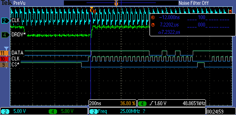
I have a problem with the SPI interface from the ADS1278.

According to the data sheet, the data MSB is ready to clock into the CPU one CLK cycle after the falling edge of DRDY*. With a 25MHz ext clock, if the SPI transfer is delayed at least 40ns after the falling edge of DRDY*, the CPU should be able to clock the MSB with the first spi clk rising edge.

But the DATA line continues to show the LSB data level from the last word transferred, all the way through the DRDY* pulse, and does not change to the new readings MSB until first falling edge of the SPI transfer. So all my readings are 1 bit behind.


Any idea what I could be doing wrong?

Thanks,

Bob

  • Hi Bob,

    Thanks for your post.

    I assume that CLK on Channel 2 is the master clock input, while CLK on Channel 10 is the SCLK for the interface? If so, then I agree that something is not correct since DATA should have shifted with the falling edge of /DRDY. And you're saying that if you shift the data one bit to the left, do the results make sense?

    What is this /CS signal that you show? The ADS1278 does not have a /CS pin.

    I do notice that the Frame-Sync Format timing diagram shows that SCLK idles high and transitions low at the beginning of the frame in line with the FSYNC rising edge to clock out the MSB. Let me confirm with a designer that it is truly the /DRDY falling edge and not the first SCLK falling edge which clocks out the MSB in SPI Format.

    Best Regards,
  • Hi Ryan,

    Thank you for your help.
    Channel 2 is the master clock. It is synchronous with the SPI clock on channel 10.
    The SPI MOSI writes to a DAC chip synchronized with the read from the ADS1278 ADC over MISO.
    The CS* on channel 9 is used for the DAC write and not connected to the ADC, it is just shown to mark the beginning and end of the SPI transfer.

    wbr,
    Bob
  • Hi Bob,

    Is the input voltage positive or negative? If it's positive, the MSB will be 0. It is possible that this coincides with the LSB of the previous data word. Can you force the input voltage to be negative, such that the MSB is 1? Then we may know for sure if there is an issue.

    I did have a designer confirm that the RTL code shows the MSB is clocked out by the /DRDY falling edge.

    Best Regards,

  • Hi Ryan,

    The original screen shot was of a single sweep trace. When you look at it while the scope is constantly re-triggering, the DATA line constantly toggles between 1 and 0 in time with the noisy LSB of the previous data word. I don't have it set up at the moment to take another screen shot, but it looks something like this. The MSB is the next bit after the rising edge of data ready, it follows the input voltage and it is rock solid without any flickering between 1 and 0.

    This is a mature chip, so I expect that your data sheet and your engineer are both correct, but it's still puzzling.

    Thanks,

    Bob

  • I tried to re-create my test this morning, and instead I found things just the way your engineer described. The data line is changing on the falling edge of DRDY* to match the MSB of the next word to transfer. By adjusting the input voltage, I can set that bit high or low.

    Thank you for your help.

  • Hi Bob,

    I'm glad you were able to confirm this on your setup. Let us know if you need anything else.

    Best Regards,