This thread has been locked.

If you have a related question, please click the "Ask a related question" button in the top right corner. The newly created question will be automatically linked to this question.

ADS131E08: DRDY hang to high level with CS fixed at low level

Part Number: ADS131E08

We developed a board with the ads131e08 but we have problems in burst test (IEC 61000-4-4) already at level 1, the data ready pin hangs at level high until we send hardware reset, we saw that if we fix the CS at low level we solve the problem but if we use it to communicate with the device during the test we experience the problem. We are using the Start pin to start the conversion and the RDATA command to retreive the result but the same behaviours is present with the CS fixed at low. Seems that the DRDY is in somehow correlated with the SPI port despite what is written on the datasheet. 

  • Hi Giovanni!

    Welcome to our e2e forum! I'm sorry to hear that you are having problems with the ADS131E08! With the given information, it's not easy to pin point what exactly the problem might be. There could be data corruption of the registers during your burst testing - have you tried reading back the registers before doing the hardware reset to verify that they are programmed the way you initially intended them to be?
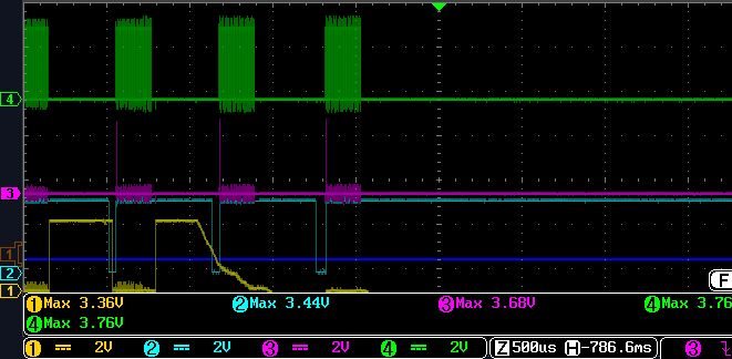
  • We investigated and we found that the configuration is mainteined, after furter investigation we discovered that the noise on the CS cause the reading of wrong data and this sometimes bring the device in different working modes, in our application every 625us we send a RDATA command and every 32 cycles we send RDATA followed by RREG command but if we fix the DIN at low level the problem is solved since DRDY is following the START pulse frequency. In the following picture is clear (CLK in green,DIN in pink, DRDY cyan, CS yellow), we kept CS (to simulate reproduce the issue) at low level ad two consecuitive RREG command lock the device since the DRDY is fixed at high level in the next cycle. The device remains lock here until we reset.
    Any advice to solve this problem? we are optoisolated and we have the pull up on the CS.

  • Hi Giovanni,

    Can you zoom in on one of those sequences so that I can get a better look at the DIN SCLK and DOUT?
  • Hi,

    i'm sorry but we don't have better acquisition where see better the DIN, SCLK, DOUT but we had isolate the problem, the device is locking because reads a different command respect what we want, this is caused by glitch on CS and DIN signal, you have any guidelines or advice to reduce the effect of the burst on the SPI communication? if we just do data read with DIN always at 0 in RDATAC mode everything works fine.

  • Hi Giovanni,

    You could add potentially add a little filtering to your SPI control lines. If you care to share your schematics, we could make suggestions.
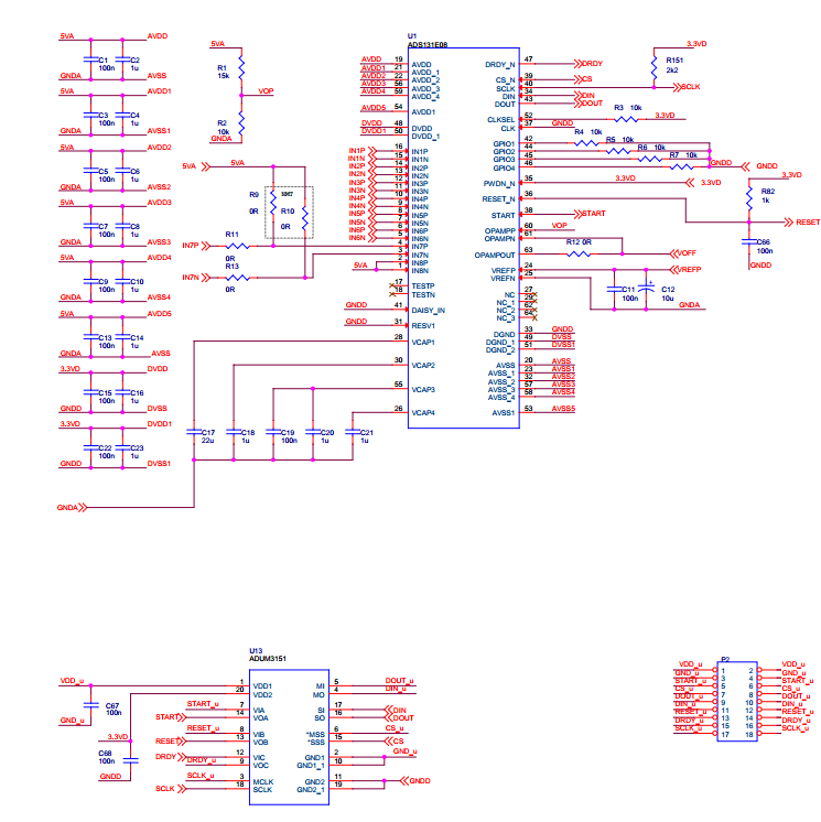
  • Here is the schematics:

  • Good morning,

    I need an urgent clarification regarding the PCB layout (ground planes and traces) near to the p/n ADS131E08IPAGR (8-Channel, 24-Bit, Simultaneously-Sampling, Delta-Sigma ADC).


    a)      In case of double layer PCB, please can you indicate the prescriptions (or a diagram) for the layout?

    b)      In case of 4-layers PCB, please can you indicate the prescriptions (or a diagram) for the layout? In this case, where is it recommended to put the 3.3V plane and the ground plane? On the external layers or in the internal layers? Please can you indicate the manufacturer recommendations?

    Please let me know as soon as possible. It’s very urgent.

    I will rest at your disposal for every clarifications.

    Best regards.

  • Hi Giovanni,

    For a two layer board, you can follow the layout example for the ADS131E08 that is in the datasheet (Figure 69). In that figure, the bottom layer would be a ground plane essentially with the top layer being used to route traces to the chip. You can see a four layer example layout in the ADS131E08EVM-PDK users guide, beginning on page 32. I also see that I never got back to you on the filtering (sorry about that) - you could add a series resistor to your CS pin on the order of 100 ohms and follow that with a 33pF capacitor to ground.
  • Good morning Tom,
    many thanks for your answer.

    Regarding the 2-layers example layout (Figure 69 of the datasheet), please can you indicate the manufacturer recommendations to realize the bottom layer?

    Regarding the 4-layers example layout in "evaluation board" datasheet (page 32 and following), please can you indicate which is the ground layer and the VDD layer for the internal layers? In order to avoid misunderstanding please indicate where put (VDD plane, GND plane and signals). Please complete below
    TOP LAYER >>>> ..............................
    INTERNAL LAYER 1 >>>> ..........................
    INTERNAL LAYER 2 >>>> ..........................
    BOTTOM LAYER >>>>.........................
    Can you indicate the manufacturer recommendations for the PCB layout?

    Many thanks for your availability.

    Please let me know as soon as possible. It's very urgent.

    Best regards.
  • Hi Giovanni,

    Most PCB design software allows you to define ground and power planes. Usually these are on inner layers, as is the case for the ADS131E08EVM-PDK. The stackup there is:

    TOP LAYER >>>> .............................. Signal
    INTERNAL LAYER 1 >>>> .......................... Ground (segmented into digital and analog areas)
    INTERNAL LAYER 2 >>>> .......................... Power (segmented into 3.3V, 5V, +/-2.5V areas)
    BOTTOM LAYER >>>>......................... Signal

    For the ADS131E08EVM-PDK, inner layers 1 and 2 are defined a 'negative planes'. What that means is everything you see in black on page 33 of the users guide is not copper - when the board is fabricated, the white areas will be electrically tied together and the black areas will be copper free, or isolated from power and ground. The black lines separate areas of primarily digital content from the sensitive analog areas of the board.

    For 2-layer boards, your PCB design package should allow you to define an area to create a copper pour or fill which you assign to a specific net name such as GND. In that case, the copper will be 'positive' and the PCB design software will know to connect the pour/fill to pins/pads associated with the defined net and clear all pins/pads that are not .

    As for specific manufacturing recommendations, that in large part is going to be governed by the end equipment/application. You can review the IPC-A-610 and/or the IPC-A-600 for more details. If it's just a generic board for general purpose lab use, you can talk with your PCB prototyping manufacturer to see if they have any specific recommendations for you that suit their own particular process environment.
  • Good morning,

    I have just an other question regarding the p/n: ADS131E08.

    On pin 28 (VCAP1) the datasheet indicates to put a 22-µF capacitor to AVSS. 

    Searching for a "0805" case format for the capacitor, I can choose between:

    a) 22uF 16V; tolerance 10%; Temperature characteristics: X5R (-55 to +85°C, ±15%)

    b) 22uF10V; tolerance 20%; Temperature characteristics: X7S (-55 to +125°C, ±22%)


    Which capacitor do you suggest to use? X5R with less tolerance but with a +85°C max temperature? Or X7S with a bigger tolerance value but with a +125°C max temperature?

    Is more important to favor the capacitance value precision or the temperature range? Take present that we need to guarantee the 55°C ambient temperature.


    Please let me know as soon as possible.


    Best regards.


  • Hi Giovanni,

    If your main concern is with the 55`C, I'd go with the tighter tolerance - the X5R option.