This thread has been locked.

If you have a related question, please click the "Ask a related question" button in the top right corner. The newly created question will be automatically linked to this question.

GND connection

Other Parts Discussed in Thread: ADC128S052, ADC124S051, LMZ13610

Hi,

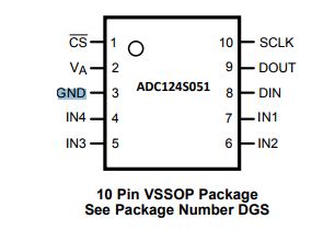
we are interfacing 2 channel ADC ADC124S051CIMM/NOPB to Joystick analog output device.

This device is supporting only one GND pin.

We are connecting ADC digital interface to FPGA.

As this device is having both analog and digital signals, which reference path  its taking ? analog GND or digital GND ?.

As per thumb rule, we have isolate the AGND and DGND.

please suggest me, whether we have to connect device GND pin to Digital GND or Analog GND.

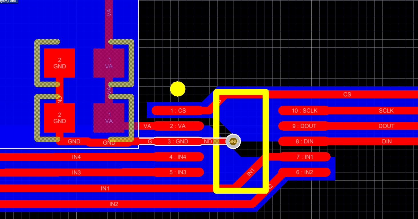
Please provide me device reference schematic and PCB guideline.

Thanks & regards,

Divya

  • Hello Divya,

    Your analog and digital ground can connect at the ground pin of the ADC124S051.  You will want a ground return path that goes between the digital pins and the the FPGA and that follows closely to these traces.  You will also want a ground return path between the inputs and the ADC124S051.  This ground path should also follow the analog lines closely.  Make sure that analog and digital lines and return paths do not travel closely parallel to each other.  You should also not cross them.  It is also acceptable to have a solid ground plane layer that connects to this pin.  Just make sure that the digital and analog lines do not travel next to each other or cross each other.  There is an example of this in the ADC128S052 datasheet, Figure 40.

    Mike

  • Hi Mike,

    Thanks for your quick support.

    sorry, i am not getting proper clarification on GND connection. ADC124S051.

    This device has only one GND pin, then how can we connect AGND and Digital GND to this device ?

    ADC128S052 - This device has separate AGND and DGND, so that we can return for Analog input over AGND and return for SPI digital signals over the DGND.

    Please guide me to understand this.

    Please provide the reference guide of ADC124S051 .

    Thanks & regards,

    Divya

  • Hi Mike,

    I want one more clarification regarding VA supply pin.
    Now we have planned to provide 5V supply as input( because analog signals source voltage is 5V), which is generating from LMZ13610 regulator In In layout side we are planing place these 2 devices far from each other.
    This idea will cause any problem to our design ?
    Please suggest.

    Thanks & regards,
    Divya
  • Hi Divya,

    It is ok if the supply is far away from the ADC.  Just make sure that you put a 0.1uF cap very close to the VA pin and also a 1uF close to the VA pin.  I have made a sample layout.  It is pasted below.

    Mike

  • Hi Mike,

    Thanks for your support.

    I have cleared on the concept of VA supply pin.

    But i want still more clarification on GND connection.

    As per attached layout example, ADC device GND is connected to Supply GND ? 

    With the same manner we also connect the ADC device GND pin to Supply GND pin. is it OK ?

    Thanks & regards,

    Divya

  • Hi Divya,

    The ADC124S051 has only one ground pin, so all the grounds (digital, supply, and inputs) need to connect to it.  You can do it like I showed in the sample layout, where you have separate analog and digital grounds and only connect them at the ground pin, or you can make a solid ground plane that is connected to the ground pin.  If you make a solid ground plane you need to make sure the return paths for the analog and digital do not cross in the ground plane.  The layout example in the previous post will also work if it was a solid ground plane instead of the separated ground planes.

    Mike