This thread has been locked.

If you have a related question, please click the "Ask a related question" button in the top right corner. The newly created question will be automatically linked to this question.

LMP90100: Need help removing offset

Part Number: LMP90100

Hello,

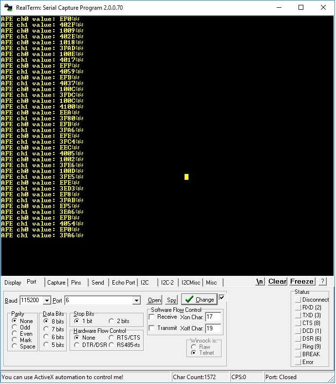
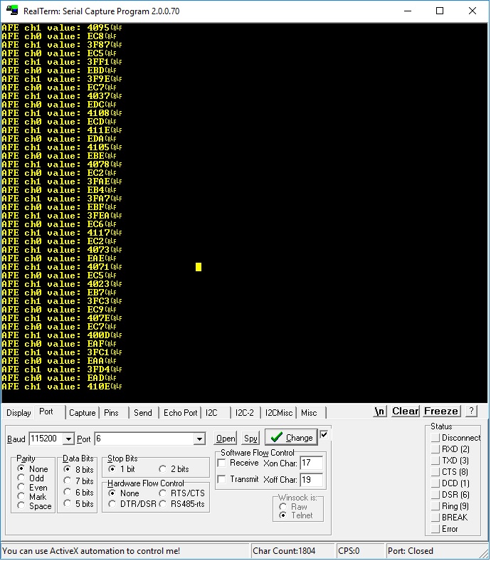
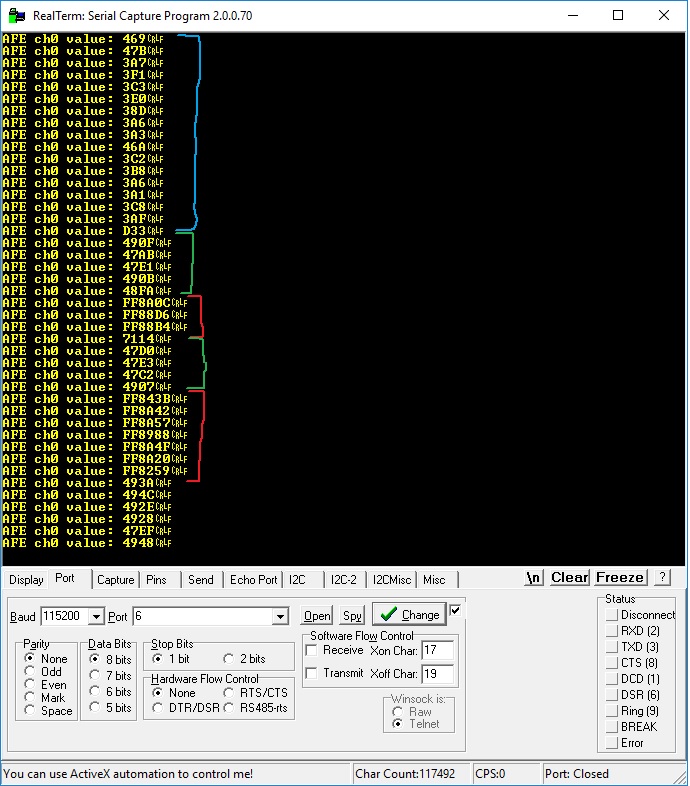
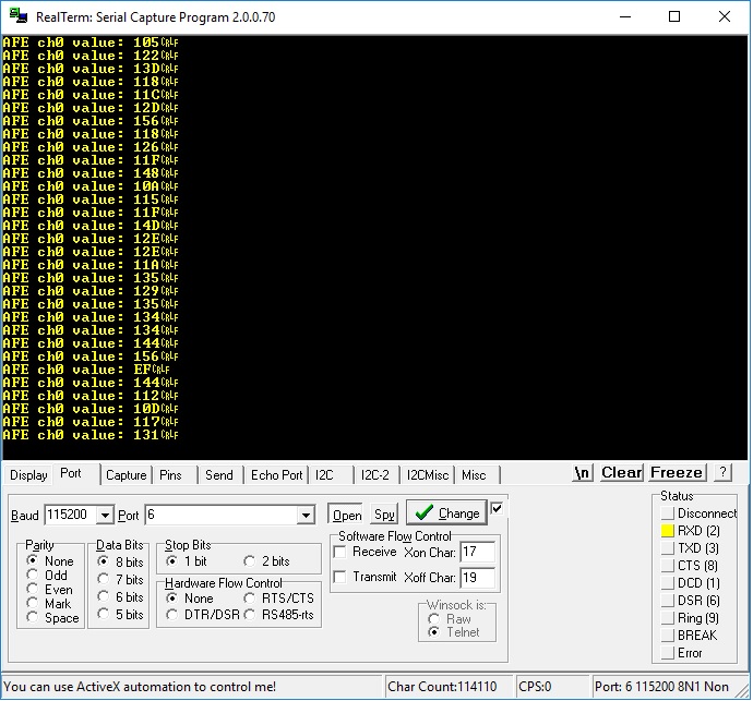
I'm using the LMP90100 in a product and I'm having a difficult time zeroing out the input.  Input channel 0 is connected to a strain gauge and when I power up the system I'm measuring roughly 0xF98.  Obviously this moves around but that is say my average value.  I'm trying to zero out the input as best as I can.  The strain gauge will have a range of +/-5mV.  I plan on using the gain available from the FGA and PGA, but if I use the gains without zeroing out the input (or getting as realistically close to zero as I can) my readings blow up because I'm amplifying this DC offset.

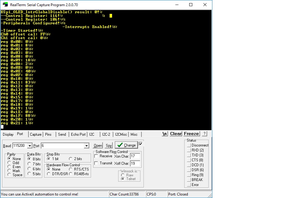
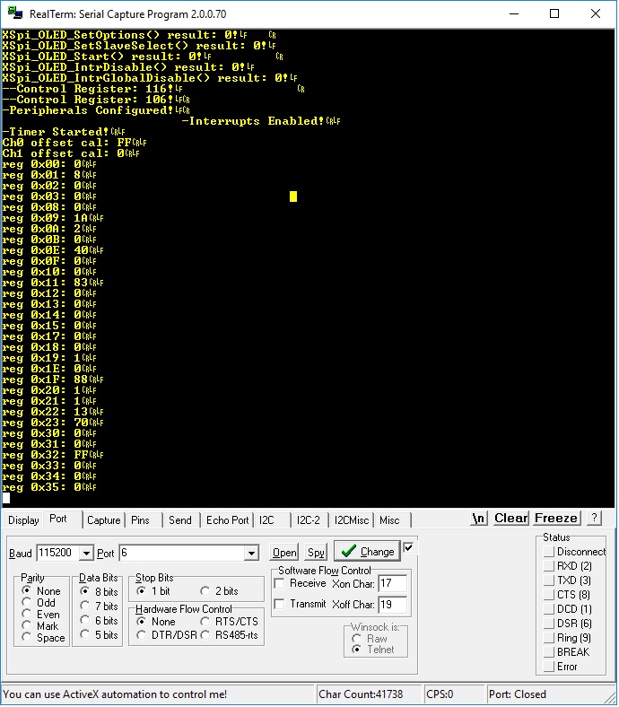
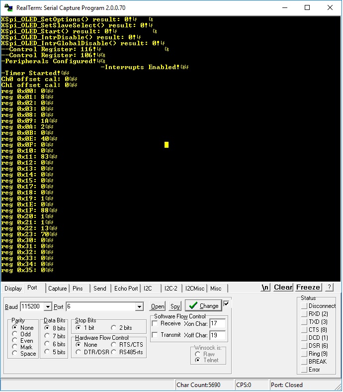
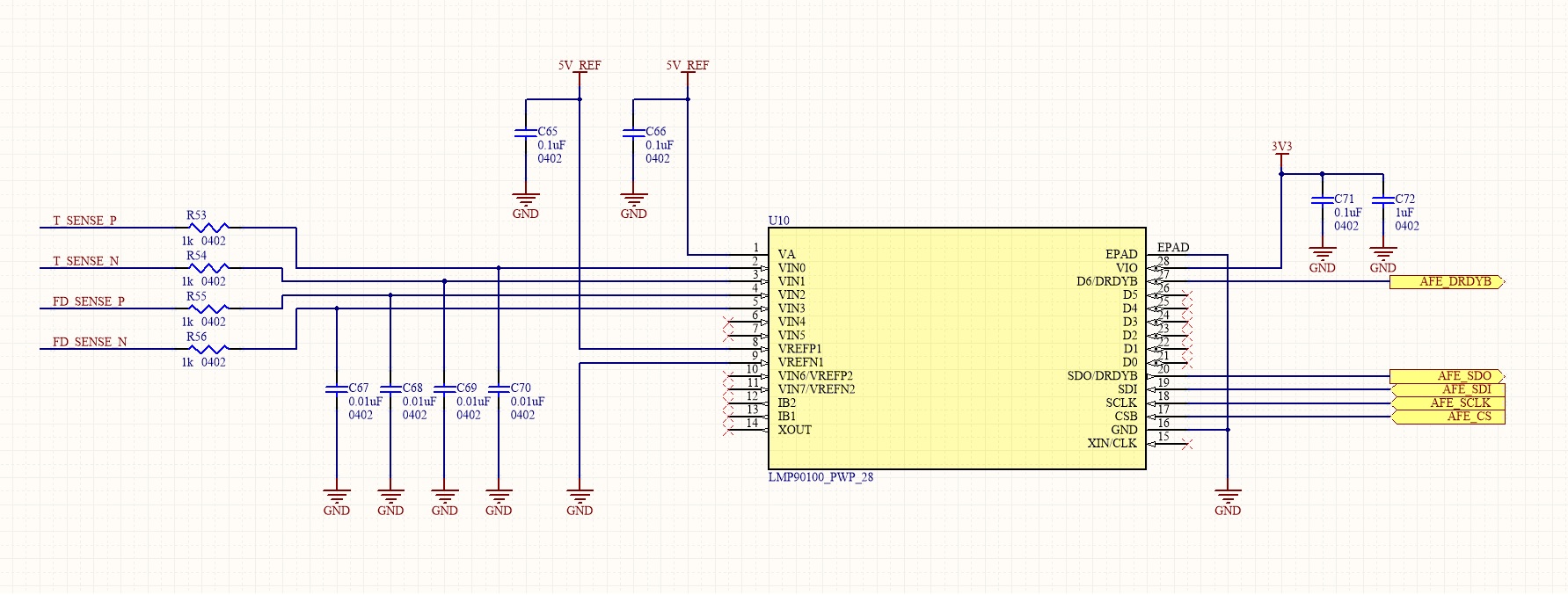
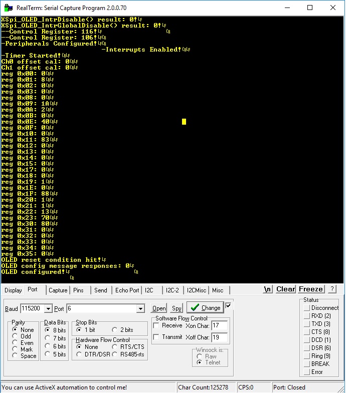
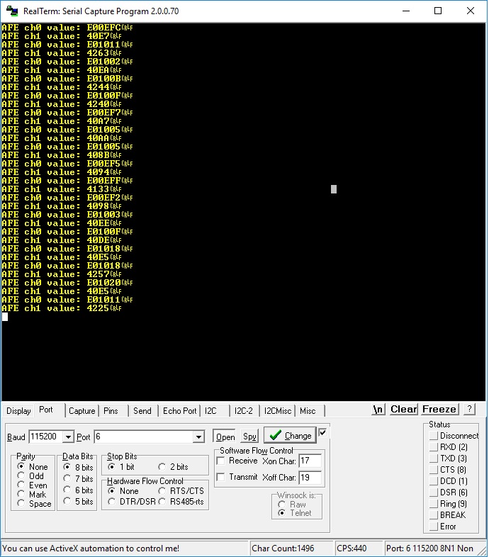
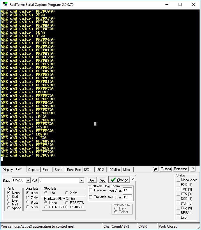
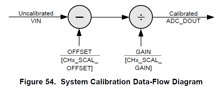
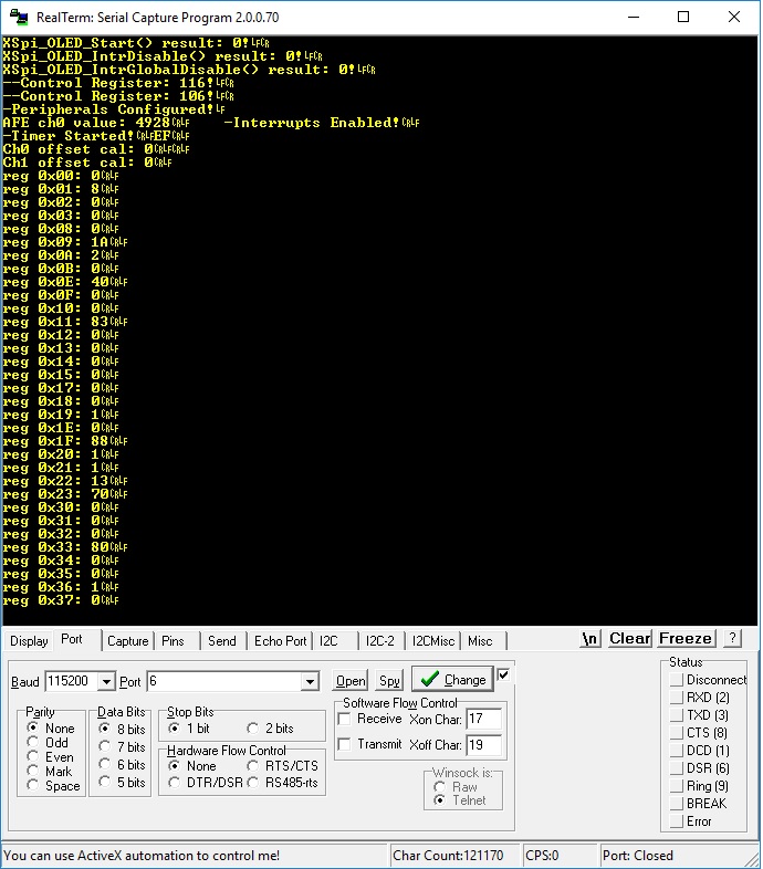
I've tried to use the "system calibration" from 9.3.7.2 of the datasheet, but when I set the CH0_SCAL_OFFSET register with ~0xF98, which is what my offset looks to be) I get ~0x1000 hex as my steady state offset.  From the data sheet I thought whatever you loaded into CH0_SCAL_OFFSET was just subtracted from your ADC sample.  All I would like to do with the embedded system is check x number of samples at power up, average them and then subtract them using the CH0_SCAL_OFFSET register.  I've read through the data sheet over and over and it seems like this should be the approach that I take, but I can't get the input to approach zero. 

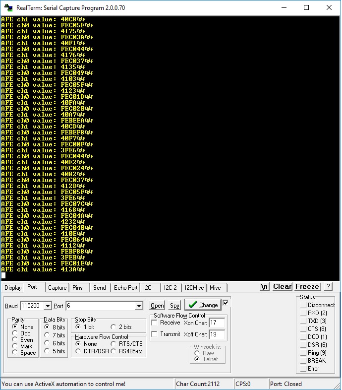
The lmp90100 is currently configured for 2x channel mode at 214sps with no gain.  channel 0 consists of VIN0+ and VIN1-.  Channel two is VIN2+, VIN3-.  I am not using any gains at the moment as I'm just trying to bring the offset down and I AM using the current buffer.  The ADC analog power is connected to a 5V high precision reference from TI as well as the strain gauge (resistive bridge).  For this testing though, I'm just driving the inputs for channel 0 with a high quality power supply.  I'm driving 2.00V into both the + and - of channel 0 and measuring the very small mismatch.  I can see the ADC functioning when I change the differential voltage between the inputs.  One direction increases with positive numbers and the other direction increases the signed output so it looks like the device is working fine.

Am I missing something?

Thanks!

  • Robbie,


    I'm not sure what's wrong, but I did have a few questions and a few things to try.

    Are you using the device in a gain of 1? Or do you change gains between the first measurement and any writing of the offset? I know that seems a bit obvious, but I thought I'd check. Do you change the gain coefficient before taking data? If you can, could you provide your configuration and how you set up the offset and gain?

    Based on Figure 54, the value stored in CHx_SCAL_OFFSET should be subtracted from the VIN coming from the ADC. However, it seems you're either getting the wrong value or the offset subtraction isn't working at all (the change between 1000h and F98h is 68h - about 100 codes).

    Instead of entering in the value directly, have you used the system calibration offset coefficient determination mode outlined in 9.3.7.2.1? This should get the correct value as well. I would run through that set of instructions and then read back the result of CHx_SCAL_OFFSET just to see if it matches what you would have gotten.

    Another test to run would be to put in a unusually large number into the CHx_SCAL_OFFSET register to see if it is being modified by gain, or used in an unusual way. If you are currently putting in F98h, put in something larger like 3E69h (4x) and see what it returns back.

    Naturally, I'd also check to see that when taking offset or running a calibration, that the offset value is really 0V in, and that there isn't some sort of inputs settling going on.

    Regardless, read through my comments, run a couple of tests and let me know how it goes.


    Joseph Wu
  • Joeseph,

    Thank you for the response!  I am using a gain of 1 (not changing from default) and I've tried writing the offset both as the first configuration message and the last configuration message.  Said differently, I've tried configuring the offset first before any other register and last after all other registers have been configured.  I have verified I can read the offset value I program into the channel 0 offset register, so if I write a FF I read an FF and if I write a 0x77 I can read a 0x77.  This seems to have no affect on the actual offset though.

    To take a step back, should I be able to read every single register in the register space and see what I've written?  If I configure all the register should I be able to read all those values back and see the exact same values I programmed in? 

    Here is what I'm programming into the registers for 2 channel (ch0, ch1) repeated sample mode.

    LMP90100 configuration register writes
    ----------------------------------------------
    0x01: 0x08
    0x02: 0x00
    0x03: 0x00
    0x09: 0x1A
    0x0A: 0x02
    0x0E: 0x40
    0x10: 0x00
    0x11: 0x83
    0x12: 0x00
    0x13: 0x00
    0x17: 0x00
    0x1F: 0x88
    0x20: 0x01
    0x21: 0x01
    0x22: 0x13
    0x23: 0x01
    0x30: 0x00
    0x31: 0x00
    0x32: 0xFF
    0x33: 0x00
    0x34: 0x00
    0x35: 0x00

    Here is what I'm reading out of those registers:

  • Here is a more complete register read:

    Here is what my data looks like with the 0xFF offset loaded as shown in the register read above:

    Here is my register reads with no offset:

    Here is the data from the no offset configuration above:

    All registers are configured in the order shown in the text list of registers and the values I'm writing to them.  I'm assuming the order in which you write to the registers doesn't matter?

  • Robbie,


    The order of the register write shouldn't make a difference.

    Right now you have the CH0_SCAL_GAIN set to 000000h. The default is 800000h. Can you keep that value set to 800000h and check the result?


    Joseph Wu
  • Also, here is the hardware configuration

  • Here are the register reads when the ch0 offset is set to 0x800000 and the read results.

    Config registers reads:

    Here are the sample results with the 0x800000 offset configured:

  • Robbie,


    I think you misunderstood. I wanted the CH0_SCAL_GAIN set to 800000h. This would be for registers 33-35. You've set the CH0_SCAL_OFFSET value to 800000h, which you should keep to near 000000h first. The offset registers are 30-32.


    Joseph Wu
  • Oh I apologize I did misunderstand.  I think this is what you were looking for.  

    Here are the register values:

    Here are the sample values:

    Why is the default value for CH0_SCAL_GAIN 0x800000?

  • Joseph,

    I think that was my mistake.  I believe what I'm getting now makes sense and the offset subtraction may be working.

    Below is my register values with no offset and sample values with no offset (I am only displaying ch0 now to make it simpler)

    Here is what I get when I set the offset value in the CH0_SCAL_OFFSET to 0x3A0.  It looks like it is subtracting.

    As a general question, does this make sense and for some basic linear lab supplies does this offset make sense?  It is not a large distance from 0V I don't think?

    1. As for acquiring data do people generally just average a lot of these values together? 

    2. There is a lot of noise.  Should I right shift to get rid of some of the lower bits? 

    3. Do you right shift until you are using the same ENOB that is described in the data sheet for my configuration?

  • Robbie,

    Thanks for making that change. I still can't tell if the offset is correct. The offset is a negative number, but it's larger than I would have expected. The output data is in two's complement notation. If I take the first output data of FEC05Eh, the result is basically negative 13FA2h, or -81826d.

    The reason I had CH0_SCAL_GAIN set to 800000 is because this value scales the gain. If you go back to the calibration diagram on page 27 in the datasheet you can see it's role in the output data.

    Normally, If you put in a full scale input (uncalibrated VIN), you would first subtract offset and then scale the output so that the full scale input yields an output data of 7FFFFF. To do this, the value for gain would also be near 800000h. Soe that 800000h/800000h is near 1. By changing this value to 000000h, it's like dividing by 0, and I'm not sure what the output data should look like. By starting with 800000h, you're starting nominally at a gain of 1 to get the output data.

    Joseph Wu

  • Robbie,


    Ok, I can now see you've gotten the device to work. I'll answer some of the answers in your last post.

    1. Averaging a lot of results isn't uncommon. It depends on what noise level people need and how much noise there is. There may also be some adjustment in data rate to make sure that line noise isn't in the result because at many lower data rates, the digital filter can handle it.

    2. I did a quick look at the results from your last photo. By taking about half of the points, it looks like there's standard deviation of about 70 codes. If you're using a 5V reference, this comes out to be about 40uV. I would compare your configuration to some of the typical characteristic curves in the datasheet to see if that's typical.

    3. ENOB is more of a statistical measurement of the RMS noise. To get ENOB use equation 17 on page 65 of the datasheet.

    Hopefully this answers your questions. Good luck on your project. If you have any further questions, you can add to this post or start another thread.


    Joseph Wu
  • Should I figure out the ENOB and drop the extra least significant bits?
  • Robbie,


    I don't really know what you're measuring so it's a bit difficult to make a determination of what you want to do. You could determine the ENOB and drop the LSBs if you want. However, you'd still have some noise in the measurement because ENOB here is a measurement of the RMS value and you might be more interested in the peak to peak value. To get something noise free, you might have to increase the RMS value by a factor of 6 (if you equate the RMS value with standard deviation, this would be 3 standard deviations from mean).

    You could also do some averaging to reduce the noise and see if you can drop the noise floor significantly. In general, with n samples, you'll reduce the noise by √n. However, you're likely to do better by reducing the data rate by the equivalent amount.

    I'd start with verifying that the noise is where it should be for the given operation. Then clean up noise sources if there are any. After that, the data is there and you can do what you want to do with it.


    Joseph Wu
  • Ok that makes sense.  I forgot to mention my setup.  I think the noise ENOB aspect makes sense now.

    My current setup is a dual output power supply driving both inputs (Vin+ and Vin- of ch0) to 2.00V with the ADC_REF at 5V.  I am trying to walk the differential voltage up in value by taking to positive input from 2.00V to 2.10V in 10mV (0.01V) increments while leaving the negative input VIN- at 2.00V.  When I step up in 10mV increments I see the output of the ADC flip from being positive to negative as shown in the image below.

    The blue is steady state with both outputs roughly at 2.000V.  The green is when I increase the vin+ by 10mV.  The red is when I increase the vin+ by another 10mV.

    I initially thought I had a noise problem, but I have some very good power supplies and am verifying their voltage outputs with a fluke meter calibrated to 1mV.  In this particular example I'm using no calibration values for the offset.

    For completeness these are the register values:

    How could the output change that much when the input is verified to be stable and separated in a postive manner i.e. the vin+ is ~20-30mV higher than vin-.

  • Robbie,


    Without knowing more about your setup, it's hard to say what is going wrong. What are you using to generate both inputs? If this is a variable lab supply, what model are you using? Are you measuring back both inputs individually? or are you measuring the differential voltage? Do you measure the voltages right at the ADC input pins? It would be worth taking some larger steps to see if there's anything else wrong.

    I took your data and converted it to voltages and the differences are roughly 10mV steps. However, they're not monotonic and not continuous:

    Data (hex) Data (dec) Voltage (mV)
    469 1129 0.67
    47b 1147 0.68
    3a7 935 0.56
    3f1 1009 0.60
    3c3 963 0.57
    3e0 992 0.59
    38d 909 0.54
    3a6 934 0.56
    3a3 931 0.55
    46a 1130 0.67
    3c2 962 0.57
    3b8 952 0.57
    3a6 934 0.56
    3a1 929 0.55
    3c8 968 0.58
    3af 943 0.56
    d33 3379 2.01
    490f 18703 11.15
    47ab 18347 10.94
    47e1 18401 10.97
    490b 18699 11.15
    48fa 18682 11.14
    ff8a0c -30196 -18.00
    ff88d6 -30506 -18.18
    ff88b4 -30540 -18.20
    7114 28948 17.25
    47d0 18384 10.96
    47e3 18403 10.97
    47c2 18370 10.95
    4907 18695 11.14
    ff843b -31685 -18.89
    ff8a42 -30142 -17.97
    ff8a57 -30121 -17.95
    ff8988 -30328 -18.08
    ff8a4f -30129 -17.96
    ff8a20 -30176 -17.99
    ff8259 -32167 -19.17
    493a 18746 11.17
    494c 18764 11.18
    492e 18734 11.17
    4928 18728 11.16
    47ef 18415 10.98
    4948 18760 11.18

    Joseph Wu

    Data (hex) Data (dec) Voltage (mV)
    469 1129 0.67
    47b 1147 0.68
    3a7 935 0.56
    3f1 1009 0.60
    3c3 963 0.57
    3e0 992 0.59
    38d 909 0.54
    3a6 934 0.56
    3a3 931 0.55
    46a 1130 0.67
    3c2 962 0.57
    3b8 952 0.57
    3a6 934 0.56
    3a1 929 0.55
    3c8 968 0.58
    3af 943 0.56
    d33 3379 2.01
    490f 18703 11.15
    47ab 18347 10.94
    47e1 18401 10.97
    490b 18699 11.15
    48fa 18682 11.14
    ff8a0c -30196 -18.00
    ff88d6 -30506 -18.18
    ff88b4 -30540 -18.20
    7114 28948 17.25
    47d0 18384 10.96
    47e3 18403 10.97
    47c2 18370 10.95
    4907 18695 11.14
    ff843b -31685 -18.89
    ff8a42 -30142 -17.97
    ff8a57 -30121 -17.95
    ff8988 -30328 -18.08
    ff8a4f -30129 -17.96
    ff8a20 -30176 -17.99
    ff8259 -32167 -19.17
    493a 18746 11.17
    494c 18764 11.18
    492e 18734 11.17
    4928 18728 11.16
    47ef 18415 10.98
    4948 18760 11.18
  • I'm using the Rigol DP832 power supply to generate both inputs. It has two adjustable outputs so I connect each of those to the channel 0 inputs. I am measuring the input voltages from the lab supply separately with two multi-meters. I'm just verifying that the positive input is increasing basically. Thanks for plotting those values out. I will be working on trying to get this part up and running reliably again this week so if you think of anything let me know! Thanks again!
  • Robbie,


    It looks like your on your way to making some good measurements. Using a lab supply as your measurements should work, but I'd be sure to use a precision multimeter to measure the input to calibrate your results. With a 10mV change, the LMP90100 should easily be able to seperate out the differences.

    The Rigol should have a low enough ripple so that the basic measurement should work with 10mV steps. Just the same, I'd still check to see what happens with larger steps.

    If you have any issues feel free to post back. Good luck!


    Joseph Wu
  • Thanks Joseph,

    I worked on this all day today.  I wanted to get your opinion on my current data.  I found an example/demo video from TI online and it looked like when connecting the two leads VIN- and VIN+  together (say for channel 0) the code read back in this video was very very low without calibration and even lower with.  I feel like the codes I'm seeing on my setup when my VIN+ and VIN- for ch0 are shorted together (the numbers seem to be the same whether I leave them floating or tie them to ground)  are high.  Below are the values I'm seeing.

    Theoretically I have this working and this is my "factory" offset.  Does this seem reasonable?  It is the same basic setup with no gains, no buffer (internal buffer amp) and running at 1.6sps. 

    Thanks

  • Robbie,


    I'm not sure about the values that you are showing. If you assume that the average value is about 110h, that would be about 272d, which translates to an offset of 160uV, assuming a reference of 5V.

    If this is the pre-calibration number then maybe this might be high, but it may not be out of the realm of possibility. I just don't have any guess as to what this value would normally be. If this is the post-calibration number, then I'd say something is wrong.

    Generally, I would short the inputs together to get the offset value also, so I wouldn't expect anything to be wrong unless there were some sort of settling issue.

    I would also note that the offset may change once the gains and buffer are enabled. If you intend on using any additional gain or buffer, I would run a calibration for that setting.


    Joseph Wu
  • That is a pre-cal number currently. I have shorted the inputs together and am using a 5V reference.

    From what I understood in the datasheet, you are supposed to try to zero out the offset as a first step when calibrating and then apply the gain. Is that correct? It sounds like you are recommending I set the gain and buffer, then attempt to zero out the offset.
  • Robbie,


    Always set the offset calibration first. If you set the gain calibration first, you'll roll in a small error from the offset into your gain calibration. Even after you've made the offset calibration, you'll get rid of your offset, but you'll retain the error that comes from the original offset in the gain calibration. It's small amount of error, but you can avoid it.

    By running the offset calibration first, your gain calibration will start with 0 offset, and then you can properly calibrate for gain.


    Joseph Wu
  • Joseph,

    I have this up and running now the offset zeroing functionality seems to be working pretty well. Now that this is working it sort of brings up a problem I didn't think about.

    Since the number is signed and when my offset is zero'd out I still have some noise that causes the number to bounce between a small positive number and small negative number. Said differently, when my strain gauge offset is zeroed out, I see the numbers at steady state fluctuate like below:


    AFE ch1 value: FFFFCE
    AFE ch1 value: 3F
    AFE ch1 value: FFFFFD
    AFE ch1 value: FFFFCC
    AFE ch1 value: FFFFB7
    AFE ch1 value: FFFFD3
    AFE ch1 value: FFFF88
    AFE ch1 value: FFFFDF
    AFE ch1 value: FFFF71
    AFE ch1 value: B
    AFE ch1 value: FFFFD0
    AFE ch1 value: 3A
    AFE ch1 value: FFFFB3
    AFE ch1 value: FFFFFB
    AFE ch1 value: FFFF76
    AFE ch1 value: FFFFF6
    AFE ch1 value: FFFFE1
    AFE ch1 value: 35
    AFE ch1 value: FFFFEF
    AFE ch1 value: FFFFF2
    AFE ch1 value: 3C
    AFE ch1 value: FFFFBD
    AFE ch1 value: 1C
    AFE ch1 value: 2E
    AFE ch1 value: FFFFE5
    AFE ch1 value: 1
    AFE ch1 value: 2B

    Just as an example. So i'm bouncing between positive and negative. Now, when I apply a gain (say of 128) this blows up on my because I get that gain applied to the negative number (which makes a much bigger negative number) and a positive number (which makes a much bigger positive number).

    How should this situation be handled? I am new to this sort of data acquisition and don't see an option with this device to deal with this. Even if my analog side was very quiet and there was very little noise, as long as the values/codes go between positive and negative it seems this issue would exist and getting exactly 0 for an offset isn't really possible.

    Do you have any guidance/recommendations?

    Thanks!
    Rob
  • Rob,


    I not sure how to answer this question. Regardless of the measurement, you'll have some amount of noise. Applying gain, you'll always gain up the noise. The trick really is to reduce the noise to as low as possible while maximizing the input signal range. This is a combination of using the data converter at a lower data rate, averaging, a clean layout, and low noise reference.

    As far as putting the device in gain and having the output code go positive and negative, you could do is truncate the output code so that the noise is smaller than the least significant bit that is visible. With a 0 input, you'd never see the negative codes.


    Joseph Wu