This thread has been locked.

If you have a related question, please click the "Ask a related question" button in the top right corner. The newly created question will be automatically linked to this question.

ADS1299: BIASOUT configuration

Part Number: ADS1299

Hi there,

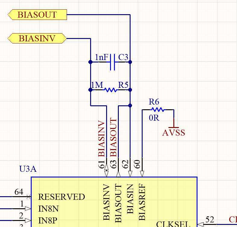
I am designing a new module that will daisy chain up to 4 ADS1299. In order to configure the BIASOUT I took as a reference the figure 38 and 39 of the Datasheet, just outputting BIASOUT and connecting BIASINV to the next ADS1299 in the daisy chain, with a resistor and capacitor to create the integrator circuit. getting the following design:
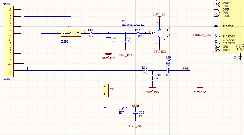
I also have a reference design from a previous project that follows a diferent strategy, putting the RC in serie and outputing the BIASINV signal through a voltage follower. Should I stick to this configuration? would it provide a better performance? 
Thank you for your help.

Best regrads

  • Hi Husein,

    Thanks for your post.

    If you are using the electrode inputs from all 4 ADS1299 devices to generate the common-mode, you simply need to short their BIASINV pins together and power down all but one BIAS amplifier. This will tie all PGA outputs to the same summing junction at the input of the one BIAS amplifier.

    It looks like your reference design is doing something slightly different. In these applications, it is common to drive the shielding around the electrodes to a common-mode potential that is close to the same common-mode present on the electrode wires themselves. This helps to reduce the parasitic coupling between the noise and reduce noise pick-up from the surrounding environment. While the BIAS amplifier is used to drive an inverted common-mode signal to the body (for better common-mode rejection), the BIASINV signal can be treated as the non-inverted common-mode needed to drive the shield. The BIASINV output should be buffered to drive the shielding so as not to place an additional load on the PGA amplifiers.

    Best Regards,