This thread has been locked.

If you have a related question, please click the "Ask a related question" button in the top right corner. The newly created question will be automatically linked to this question.

ADS1220: Problems with output data

Part Number: ADS1220

Hello!

I'm working with ADS1220 - SPI version.
The configurations are default.
I'm sending SYNC command and when data is ready on DRDY signal I'm receiving data and showing it to the terminal. The data is also controlled by logic analyser on MISO pin.
I'm connecting 1.5V battery in differential mode to check system.
After start all is good: the result is about 6 200 000 in DEC, that is similiar to ~1514 mV. But some time later (some minutes) system starts to show maximum value 8 388 608, that is displaying on logic analyser and on the terminal. When I'm disconnect battery and connect input pins tougether the result is nearby 0. But when I'm connect battery back the result is again goes to maximum. The system works in the same way arfter hard reset again and again.

Do you have any ideas?

Regards,
Vlad

  • Hi Vlad,

    Welcome to the E2E forum! To help us understand your setup a little better could you tell us which ADS1220 inputs you are using and the ADS1220 register settings? Also, are you directly reading the data or using the RDATA command? It would also be helpful to see your logic analyzer shots. For the shots please include DRDY as well as the SPI signals. Do you have a schematic you can send as well? In particular I would like to know what supply voltages you are using for DVDD and AVDD/AVSS and how they are being derived as well as any input filtering being used.

    If you are using the default register settings, something you could try is to disable and bypass the PGA (Register 0, bit 0). You could also try and measure the voltage referenced to analog ground by connecting the battery minus to AGND (AVSS) and then using the mux connection to measure single-ended. As it does appear that the voltage input is floating to something outside of the input range, one of the above steps may help in determining what might be actually happening.

    Best regards,
    Bob B
  • Hello Bob,

    Thank you very much for the fast response! The problem was pretty simple: just some bugs in code. But now I have more serious problem.

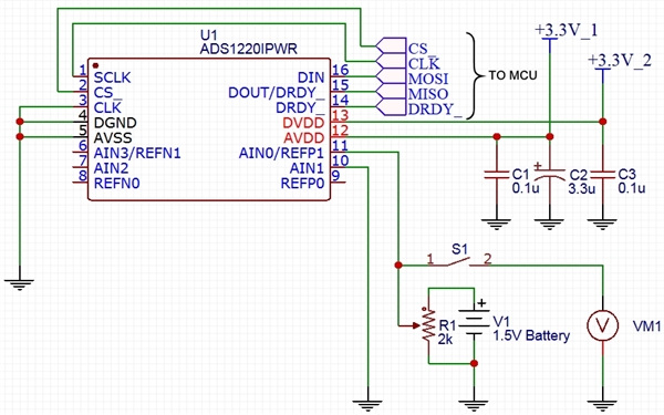
    Firstly, I should show circuit:

    So, I have two + 3.3V LDO voltage sources (VS). The first VS (+ 3.3V_1) is connected to AVDD. I use 0.1uF ceramic capacitor and 3.3uF tantalum capacitor as far as close to AVDD pin. The second VS (+ 3.3V_2) is loaded by DVDD and MCU.

    Secondly, about registers configuration.
    R [0] == 0x00;
    R [1] == 0xA0;
    R [2] == 0x00;
    R [3] == 0x00;

    Thus I'm working in a single shot mode with differential inputs on AIN0 and AIN1 at 600SPS.
    I'm sending START / SYNC command and waiting until DRDY_ will go low. Then I'm receiving data in terminal as decimal (DEC) - now without artefacts :)

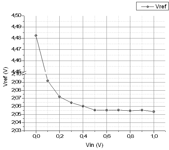
    I have collected practical values of Vref depending on input voltage Vin=AIN0-AIN1. I'm using following expression: Vref=Vin*(10^23)/DEC. Before DEC fetching I turn on S1 and fixing Vin by voltmeter with 0.1% accuracy.
    In the plot below average values of Vref were shown (20 samples per one dot).

    The result is very bad: especially at low Vin. It's clear, that Vref calculation at Vin ~ 0 is unfairly, but at Vin >= 0.1V the values are reliable.

    Do you have any ideas?

  • Hi Vlad,

    I'm glad to hear that you have made some progress.  What you are currently trying to do is not clear to me.  The internal VREF of the ADS1220 is 2.048V and the reference specifications are given on page 7 of the ADS1220 datasheet in the Electrical Characteristics table.  Normally you would measure an input voltage using the ADC, but apparently you are trying to indirectly calculate the internal voltage reference.

    There are a couple of issues with your measurement.  The main issue is you are violating the common-mode input voltage specification when using the PGA enabled.  Please see section 8.3.2.1 starting on page 22 of the datasheet.  AIN1 connected to AGND violates the specification with PGA enabled.  To make single-ended measurements you must disable and bypass the PGA by setting bit 0 of the Register 0 to '1'.

    Other issues relate to noise and aliasing.  You should add an RC low-pass filter to the AIN0 input to avoid any noise pickup from cabling/wiring as well as provide an antialiasing filter.  I would keep the R value less than 2k ohms and you could start with a capacitor of 10nF to 100nF.

    Best regards,

    Bob B