This thread has been locked.

If you have a related question, please click the "Ask a related question" button in the top right corner. The newly created question will be automatically linked to this question.

ADS131A04: Problems with Spurious Tones / Limit Cycles

Part Number: ADS131A04
Other Parts Discussed in Thread: INA827, TM4C1294NCPDT

Dear all,

I'm using the ADS131A04, 4-channel delta-sigma ADC, in a strain gauge amplifier design. For my application, 12 channels are required in total but board area is limited so I designed a small stackable board with 4 channels. Three of those boards are plugged into a main circuit board with a TM4C1294NCPDT for signal processing. Reading out the ADCs via SPI works perfectly fine. However, on inspection of the signals I noticed odd disturbances on all 4 channels of some ADCs in the form of low frequency oscillations that occur periodically every couple of seconds. The signal swings up to of 0.5-2mVpp and then fades out again. As the measured signals from the strain gauge amplifiers (INA827) are also on the mV level, such a disturbance is undesirable. Due to its nature, I believe it is also impossible to filter.

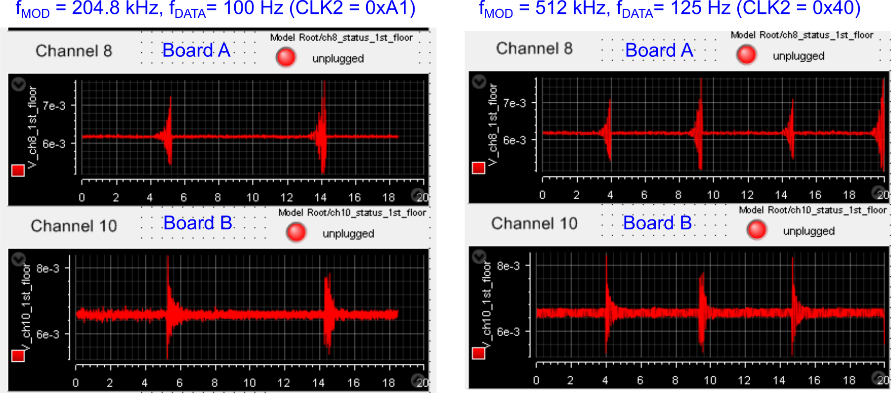
I suspect that what I'm seeing are spurious tones / limit cycles of the delta-sigma ADCs. This is because when I change the modulator sampling rate of the ADS131, the number of disturbances I get in a given period scales accordingly. When changing the ratio of modulator to output sampling rate, the characteristics of the disturbance change. Y-Axis in the figure is in V, time scale in seconds.

Given that my assumption is correct, there still are a couple of effects that I do not understand:

  1. When plugging in only one of the small boards on the main board, the disturbance never occurs.
  2. One out of 3 boards does never shows the disturbance for any possible combination of individual boards on the main board.
  3. Combining one of the "bad" boards with the "good" one leads to a different form of disturbances.
  4. Combining the two "bad" ones always produces the disturbance I discribed, but the characteristics change a little bit depending on which sockets I use on the main board.
  5. As you can observe in the pictures, the disturbance is shifted in time between boards and somehow "mirrored"

1) might be explained by the overall noise level changing due to the increase of supply current / capacitance when adding another board.

2) is possibly due to variation in the production process (?)

As for the other effects, I have no idea. Any suggestions/help/comments are greatly appreciated. I need to know the origin of the disturbance and a strategy to avoid it before manufacturing more PCBs that end up being useless for my application.

Input to each positive ADC channel comes from the output stage of a INA827 instrumentation amplifier. Negative inputs are tied to ground. AVCC/AVSS and IOVDD/IOVSS of the ADS131 are tied to the same supply. An (unbuffered) external voltage reference, REF5045, is used. Relevant parts of the schematic are attached for your reference.

Since this is my first post, I hope that I provided all the necessary details. If you need to know anything else about the circuit, system setup, power supply or other stuff, please let me know.

schematic_small_board_ina.pdf

  • Forgot to upload the ADC schemactic, sorry. schematic_small_board_adc.pdf

  • Hi Alexander,

    Thanks for your interest in our ADS131A04!

    At first glance, it looks like something from the interface side is coupling onto the analog inputs, whether it's the master CLK input, /DRDY, SPI lines, or something else. Just to rule out some possibilities, are you doing anything other than reading data during these captures (i.e. checking a register)?

    I'll take a closer look at your schematic and see if I can come up with other suggestions.

    Best Regards,

  • Hi Alexander,

    I've thought of a few more questions:

    How is CLK1 configured in both cases? For fDATA = 100 Hz, I assume CLK1 = 0x04? For fDATA = 1 kHz, your internal clock (fICLK) would be running at 1 kHz * 4096 * 4 = 16.384 MHz (CLK2 = 0x40). However, your external clock shows 16.384 MHz. Please keep in mind that the maximum fICLK is 12.5 MHz and the minimum ratio between fCLKIN and fICLK is 2 for CLK1[7:5].

    When you connect multiple boards to the TIVA main board, how are your sharing the grounds? Are they star-connected back to a common point on the main board?

    Also, are you reading the data in parallel through a separate interface for each ADC, or are you daisy-chaining the devices together? Does the issue follow the ADC board, or does it follow the port you use to connect to the TIVA main board?

    Best Regards,
  • Hi Ryan,

    thank you very much for your reply!

    CLK1 is 0x04 in both cases, so in the second case, fMOD = 512kHz  and fDATA = 125 Hz, sorry about that.

    The grounds are connected via the bottom layer ground plane of the TIVA main board.

    Each ADC is read out using a separate SPI interface. Data reading is triggered by the !DRDY pin and no other ADC registers are set/read during sampling. The issue occurs only for 2 out of 3 boards, regardless of the port I use on the TIVA main board. It does, however, show slightly different characteristics (frequency of the distortion, periodicity and amplitude) depending on the port. I tried all possible combinations on the TIVA main board.

    Best Regards,

    Alexander

  • Update:

    I swapped the ADC of one of my boards that never showed the disturbance I described with the ADC of a "noisy" board.
    The noise remains localized on the board so there's probably nothing wrong with the ADC itself and the disturbance I observe is not caused by limit cycles (?).

    I guess the issue is incorrect layouting, especially with respect to grounding. The small boards have 2 ground planes (one on the top and one on the bottom layer). They connect to the TIVA main board ground plane via pin headers on both the top and the bottom side of the board.

    Not being a professional PCB designer, the layout is definitely far from ideal. But could that be the issue? Can grounding problems cause the disturbances I observe or do you think it is something else?

    I can also upload the layout for you to check if neessary.
  • Hi Alexander,

    I'm glad you've found some clues about the root cause! PCB layout can definitely introduce strange anomalies in your system, especially grounding. Are the PCB designs different between the two boards?

    If you are using ground planes on the top and bottom layers, you should "stitch" them together with vias in multiple places to keep their potentials as close as possible. Do you also have an internal ground plane? Using an internal ground plane can also help improve noise performance, especially if that layer remains largely intact and uninterrupted by other traces.

    The routing of high frequency signals, such as clocks and interface lines, also plays an important role. Try to keep these signals as separated from sensitive analog circuitry as possible. Small R-C filters on these signals can sometimes help by slewing the signal edges a little and removing the higher frequency content.

    Increasing decoupling capacitors on the analog and digital supplies is another approach to quieting down noisy systems. In your next layout, try to make provisions for additional decoupling caps. I usually use a smaller 0.1uF cap directly next to each supply pin, plus 1uF caps nearby for analog and for digital supplies.

    Regarding the possibility of limit cycles, I don't believe we expect or have ever observed such a phenomenon with the ADS131A04.

    Best Regards,