This thread has been locked.

If you have a related question, please click the "Ask a related question" button in the top right corner. The newly created question will be automatically linked to this question.

ADS9120: Problem connecting negative analog input to Gnd

Part Number: ADS9120

Dear TI Community,

 I'm new here and have a question.

I am trying some things out with the ADS9120 Evaluation Module.

I have removed the input driving path and connected two wires to the analog inputs of the ADC.

After connecting a battery to the inputs I could see the 3V.

Connecting the two input pins directly with each other also worked fine. The ADC returned a zero.

The problem:

I connected the two inputs with each other and also with GND of the board. The ADC returned a constant 22369 (about 3.4V).

Does anyone understand this behavior?

Thanks in advance

Eric M. Diederich

  • Hi Mirko,

    Welcome to the E2E forum.

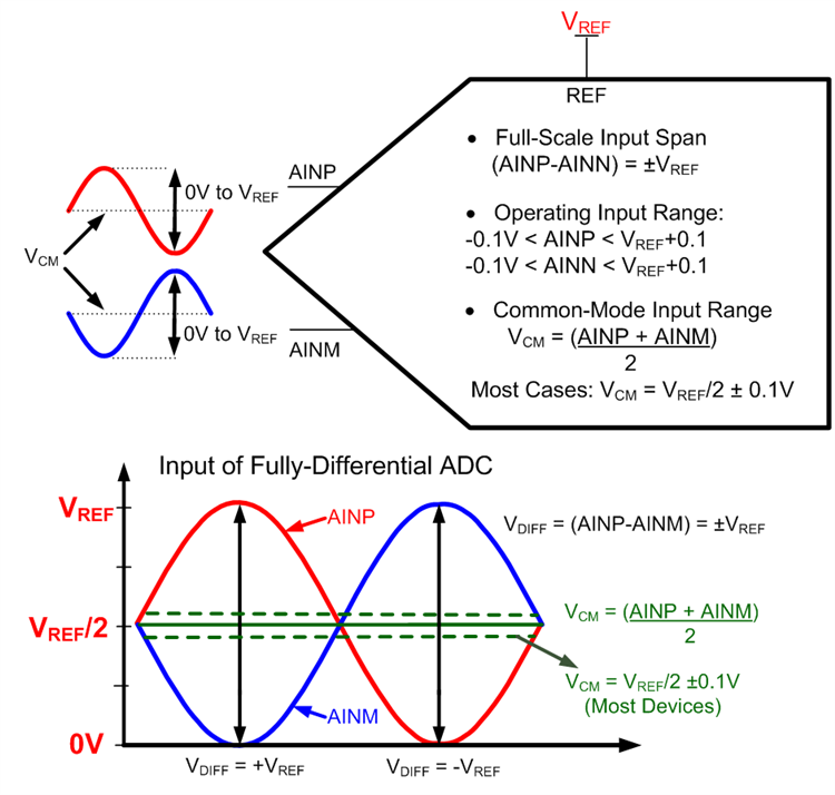
    The ADS9120 is a SAR ADC with fully-differential inputs, and converts the difference between the negative (AINM) and positive (AINP) inputs.  However, most  Fully-differential SAR ADCs have an input voltage common-mode (VCM) range specification. VCM is defined as the average voltage between the positive and negative  inputs of the ADC:

    VCM = (AINP + AINM) / 2.

    In the case of the ADS9120, the allowable common-mode voltage requirement is VREF/2 +/- 100 mV.  Please see figure below:

    In the case of the ADS9120EVM board, the reference voltage is VREF= 5V, where the ideal common-mode voltage is 2.5V, allowing a common-mode voltage range between 2.4V to 2.6V.  When connecting the Positive ADC input (AINP) to the positive terminal of the +3V battery, and the negative input (AINM) to GND,  the common-mode voltage is 1.5V which is outside the common-mode range; and the device is outside of its linear region of the ADC; and therefore the ADC does not operate properly.

    In addition, SAR ADC inputs are not high-impedance, and in most applications, unless you are using the ADC at very slow data rates, they need to be diven with a relative high bandwidth amplifier (or a  low impedance source circuit), where the driver circuit needs to be able to charge the internal sample-and-hold of the SAR ADC. The figure below shows two possible amplifier circuits that allow you to drive the differential inputs of the SAR ADC:


    One big benefit of the fully-differential amplifier (FDA) is that the output common-mode voltage can be controlled independently of the differential voltage using the VOCM input pin.  You could consider using an FDA such as theTHS4551 to drive the ADS9120.

    We have some tutorial videos and collateral that explain this topic.  The TI Precision Labs ADCs: SAR Input Types tutorial discusses the types of inputs on different SAR ADCs:

    https://training.ti.com/ti-precision-labs-adcs-sar-adc-input-types

     Please see the video, driving a SAR ADC with a fully differential amplifier:

    https://training.ti.com/ti-precision-labs-adcs-driving-a-sar-adc-with-a-fully-differential-amplifier

    For detailed theory, explanation and simulation examples on SAR ADC input amplifier driver design please also view:

    https://training.ti.com/ti-precision-labs-adcs#section-5

    Please let me know if you have additional questions,

    Many Thanks,

    Luis Chioye

    Precision ADC Applications