Greetings
I am having trouble routing the CLKOUT signal from the ADC board to the ZC706 board and using it as a clock.
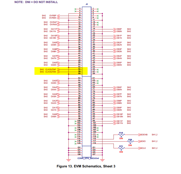
The pins I am interested are shown here on the evm,
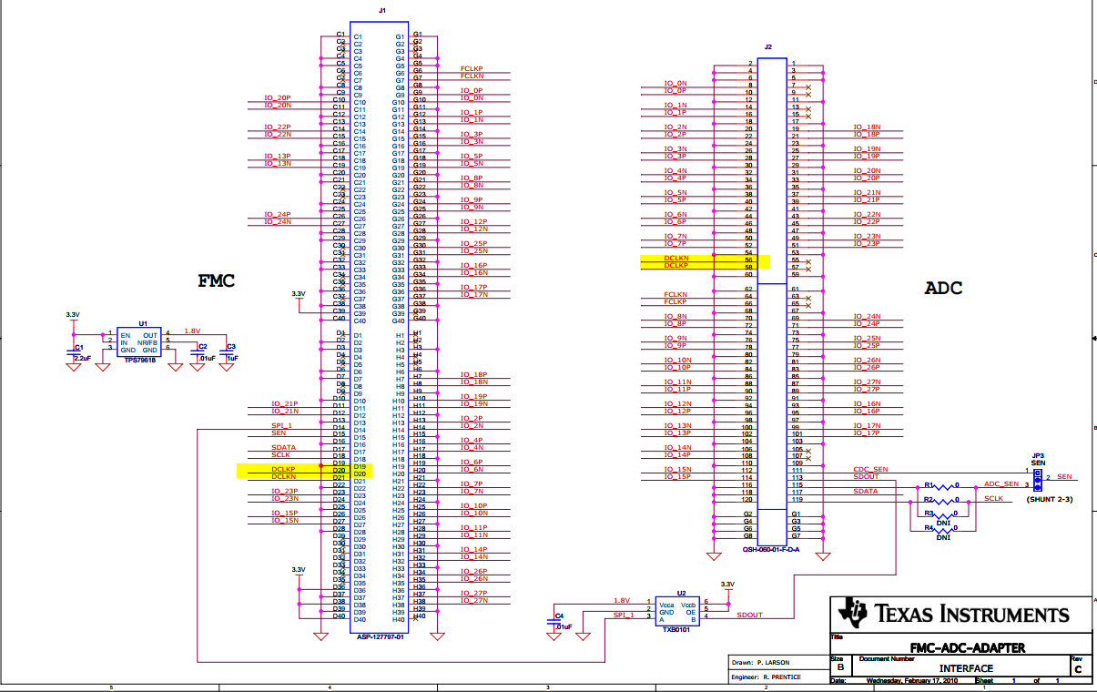
Then routed to the FMC ADC adapter board
Which routes to a non-clock pin on the ZC706
V23   IO_L24P_T3_13            3                  13    NA            NA                  HR        NA
W24   IO_L24N_T3_13            3                  13    NA            NA                  HR        NA

However the DA5(on the EVM) does route to a clock capable pin,

Is my understanding of all this correct?

I my intention was to drive my FPGA with the the output clock from the ADS board.

Thank you!

-Emil C


