This thread has been locked.

If you have a related question, please click the "Ask a related question" button in the top right corner. The newly created question will be automatically linked to this question.

ads1258: problems getting readings using Channel Data Read Command (register format)

Part Number: ADS1258

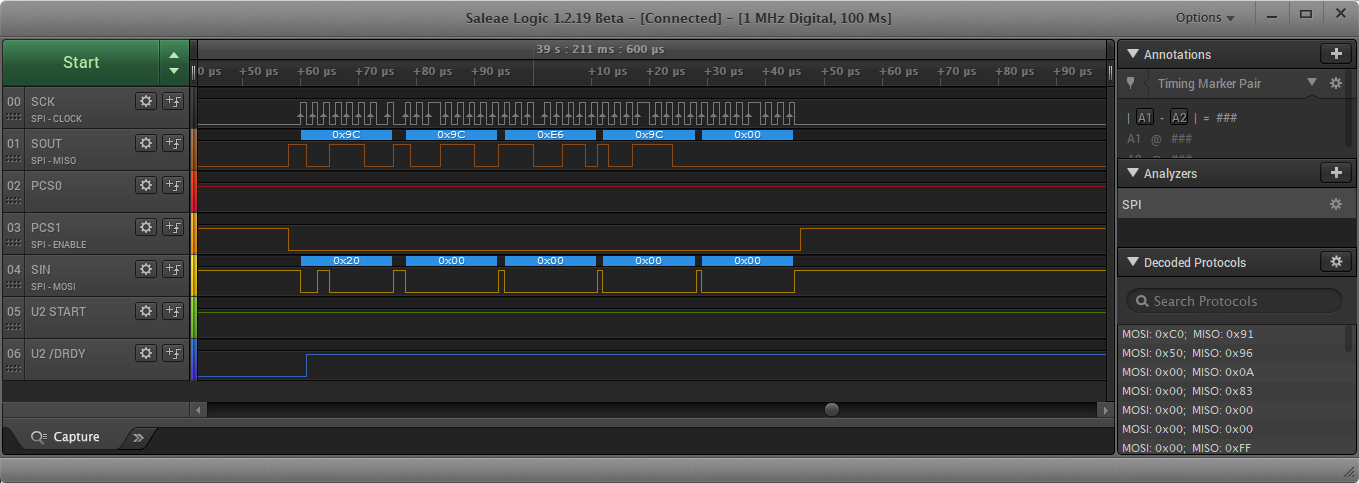
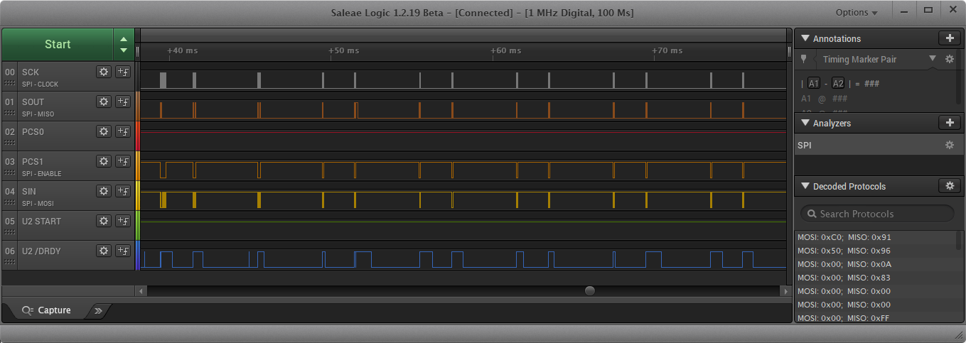
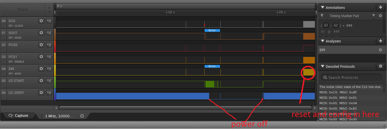
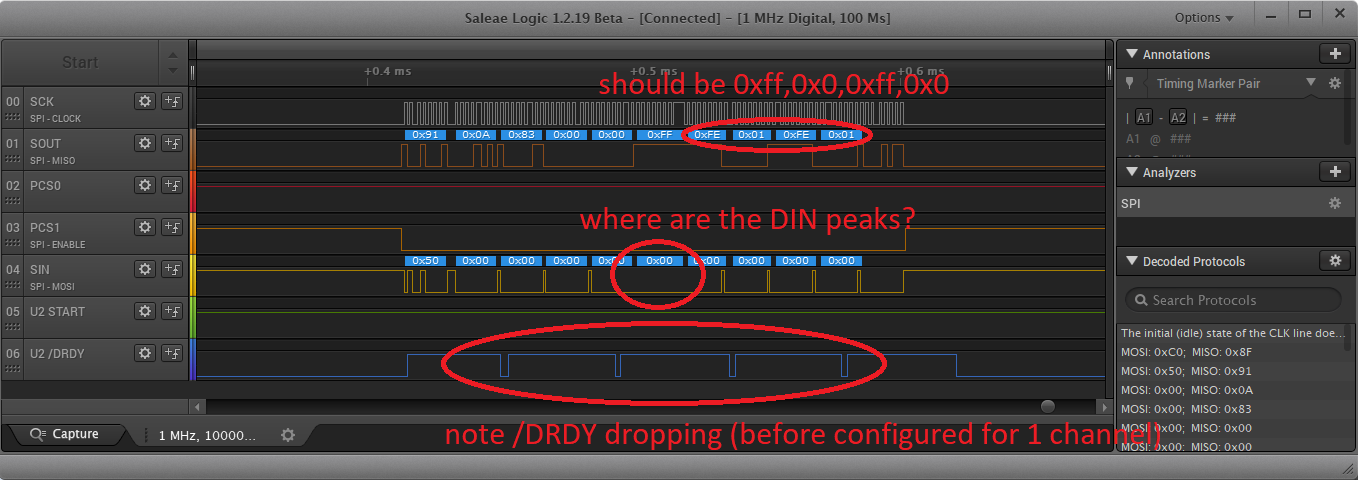
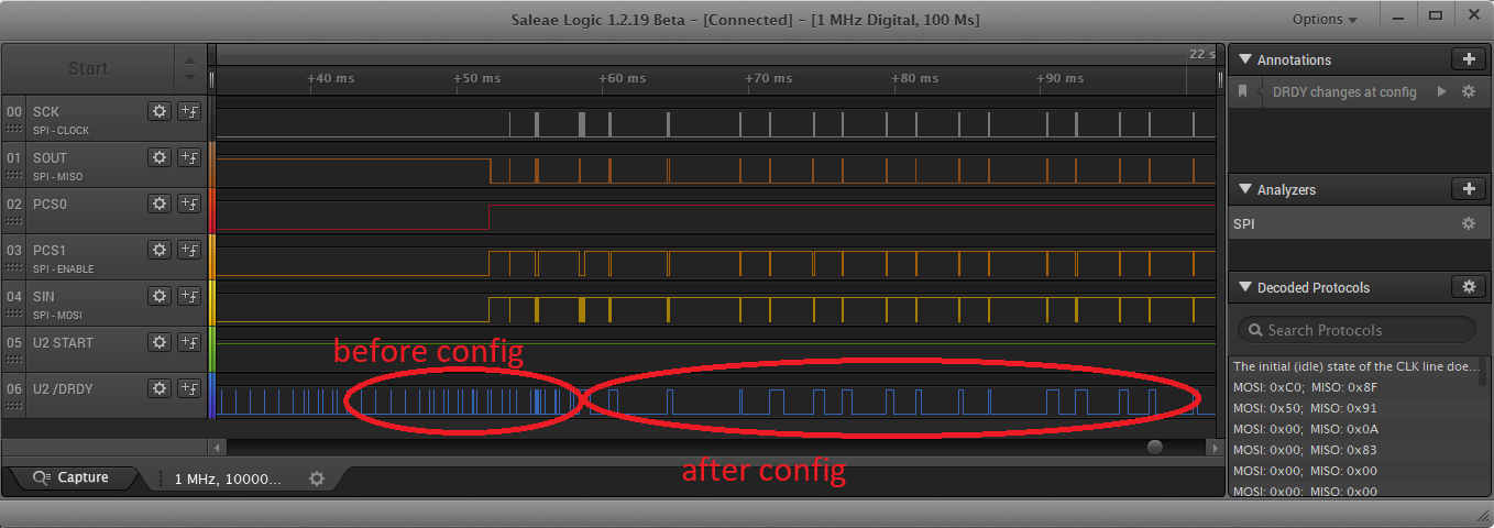
/DRDY not connected so can't use it.

START tied high

simply want to read 16 single ended A/Ds about every 10 msec so trying to figure out how to get close to this behavior

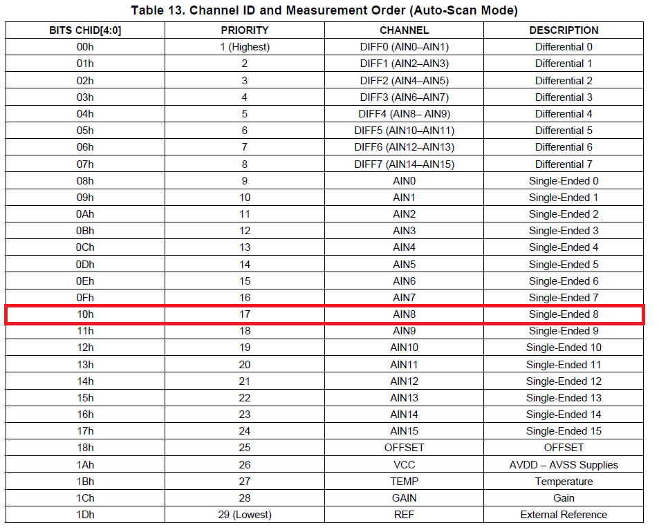
config regs set to (and verified) 0x02,0x70,0,0,0x00,0x01,0,0,0 (status byte on, max delay, only AIN0 enabled)

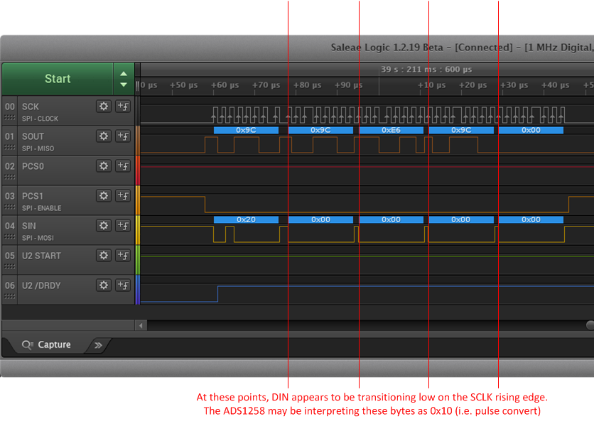
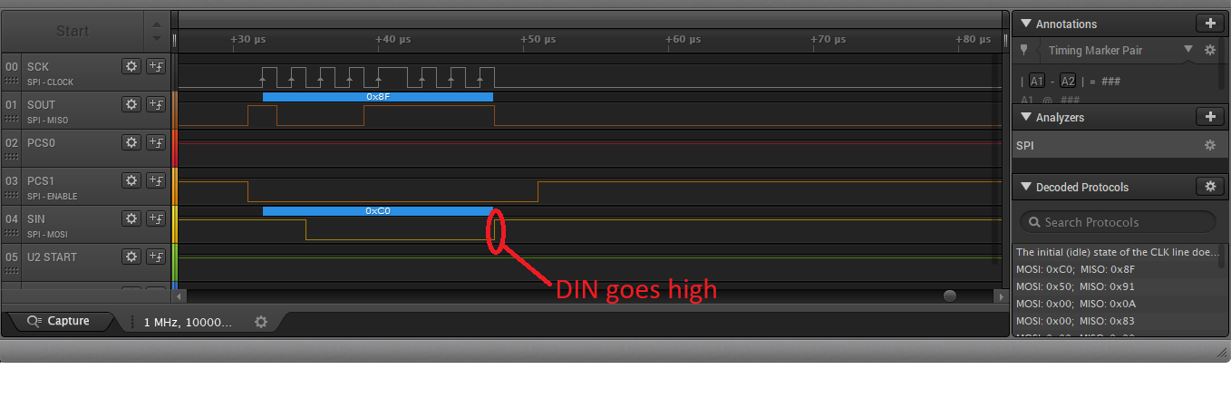
when I read channel data via register format, I get NEW 16. That's it. Why not NEW 8?

Once I have this one channel working I'll change registers to read the rest as well

I have more questions once this is straightened out

  • Hi Mark,

    Welcome to the TI E2E Forums!

    Are the CHID[4:0] bits of the STATUS byte = 16 (10h)?
    According to Table 13, you are getting the correct value that corresponds to AIN8. The values are not mapped 1:1 to the various inputs, as shown below...


    Best regards,
    Chris

  • Thanks Chris. 

    Yes, I have discovered that The values are not mapped 1:1 .

    But my config register selection has AIN0 turned on. Why would I get AIN8 readings?

  • Oops. After giving that answer, I looked again and see I'm getting exactly what I asked for...AIN8. Thanks for looking over my shoulder Chris...
  • No problem, let me know if there is anything else I can help with!

    BR,
    Chris
  • Turns out there is Chris. I am getting readings from AIN8 but don't understand how to interpret them.
    Here are some examples:
    0x88,0x07,0xfe,0xfe
    0x88,0xe6,0x21,0x00
    0x88,0x3c,0xe3,0x00
    0x88,0x70,0x16,0x00
    0x88,0xe3,0xcd,0x00
    0x88,0xe6,0x21,0x00
    0x88,0x97,0x05,0x00
    0x88,0xe6,0x3f,0x00
    0x88,0xe6,0x24,0x00
    0x88,0xfb,0xff,0x00
    0x88,0xf9,0x7b,0x00
    0x88,0xe6,0x35,0x00
    0x88,0xee,0x59,0x00
    0x88,0x37,0x03,0x00
    0x88,0xe3,0xcc,0x00
    0x88,0xe3,0xef,0x00
    0x88,0x7a,0x03,0x00
    0x88,0xb7,0x98,0x11
    column 1 is the status byte, column 2 is the MSB (AFAICT), column 3 is MSB -1 and column 3 is LSB.
    There is nothing present on the input so it should not be changing but it is. Makes me wonder if I have everything setup right. It looks like garbage.
    But if any row of that data is 2's complement, it is a really large number. How? e.g.: 0xb7,0x98,0x11... 0xb79811...0x4867ef again a very large number. this does not make sense.
  • reading the ref channel also produces erratic data:(last 3 columns are the data MSB,MSB-1,LSB)
    NEW 29:0x9d,0xc5,0x05,0x9e
    NEW 29:0x9d,0xcf,0x0a,0x00
    NEW 29:0x9d,0x8f,0xf3,0x00
    NEW 29:0x9d,0x99,0xe1,0x00
    NEW 29:0x9d,0xcf,0x3f,0x00
    NEW 29:0x9d,0xcf,0x67,0x00
    NEW 29:0x9d,0xfc,0x90,0x00
    NEW 29:0x9d,0xcb,0xfc,0x00
    NEW 29:0x9d,0xcf,0x97,0x00
    NEW 29:0x9d,0xbe,0xf1,0x00
    NEW 29:0x9d,0x8c,0x81,0x00
    NEW 29:0x9d,0xcf,0x38,0x00
    NEW 29:0x9d,0xcd,0x36,0x00
    NEW 29:0x9d,0xee,0x0f,0x00
    NEW 29:0x9d,0xcf,0x9c,0x00
    NEW 29:0x9d,0xcf,0x78,0x00
    NEW 29:0x9d,0x7d,0xe7,0x00
    NEW 29:0x9d,0x60,0x7d,0x01

  • Hi Mark,

    What is your reference source and voltage? Have you tried reading the supply or gain channels?

    Without an input voltage, the ADC inputs will float and may result in random output codes. The reference channel reading will do the same if you don't have an external reference voltage connected and enabled. Have you tried the other internal monitor channels, they should provide more stable results (though due to noise you should expect to see some small fluctuations).

    Best regards,
    Chris

  • OK Thanks Chris. That will likely resolve my issue. I'll let you know...

  • OK Chirs, I tried 4 internal monitor channels and the data is below. I am getting seemingly random data. By the way the ref data above should have been good because we have a 4v ref connected.

    the first row below is internal monitor channel name, 2nd row is default config after reset, 3rd & 4th row is 2x query of config after setting for verification. then the NEW means the new bit in the stat byte and the xx: is the chid channel number from stat byte followed by the raw hex bytes of the 24 bit reading followed by MSB and MSB-1 converted to 16 bits and converted to decimal (subtract 1, invert bits). see anything wrong?


    offset:
    0x0a,0x83,0x00,0x00,0xff,0xff,0x00,0xff,0x00,0x8b,
    0x02,0x70,0x00,0x00,0x00,0x00,0x01,0x00,0x00,0x8b,
    0x02,0x70,0x00,0x00,0x00,0x00,0x01,0x00,0x00,0x8b,
    NEW 24:0xff,0xff,0x9c,65536 (0x10000)
    NEW 24:0xff,0xb1,0x00,20224 (0x4f00)
    NEW 24:0xff,0xe3,0x00,7424 (0x1d00)
    NEW 24:0xff,0xba,0x00,17920 (0x4600)

    vss:
    0x0a,0x83,0x00,0x00,0xff,0xff,0x00,0xff,0x00,0x8b,
    0x02,0x70,0x00,0x00,0x00,0x00,0x04,0x00,0x00,0x8b,
    0x02,0x70,0x00,0x00,0x00,0x00,0x04,0x00,0x00,0x8b,
    NEW 26:0x8e,0xe5,0x9e,7471104 (0x720000)
    NEW 26:0x95,0x97,0x00,6973696 (0x6a6900)
    NEW 26:0x6a,0x8c,0x00,9794560 (0x957400)
    NEW 26:0x93,0x57,0x00,7121152 (0x6ca900)

    temp:
    0x0a,0x83,0x00,0x00,0xff,0xff,0x00,0xff,0x00,0x8b,
    0x02,0x70,0x00,0x00,0x00,0x00,0x08,0x00,0x00,0x8b,
    0x02,0x70,0x00,0x00,0x00,0x00,0x08,0x00,0x00,0x8b,
    NEW 27:0x60,0x9a,0xf7,10485760 (0xa00000)
    NEW 27:0xd7,0x79,0x00,2656000 (0x288700)
    NEW 27:0xbd,0x8d,0x00,4354816 (0x427300)
    NEW 27:0xd7,0xa7,0x00,2644224 (0x285900)

    gain:
    0x0a,0x83,0x00,0x00,0xff,0xff,0x00,0xff,0x00,0x8b,
    0x02,0x70,0x00,0x00,0x00,0x00,0x10,0x00,0x00,0x8b,
    0x02,0x70,0x00,0x00,0x00,0x00,0x10,0x00,0x00,0x8b,
    NEW 28:0x77,0xf4,0x18,8978432 (0x890000)
    NEW 28:0xf4,0x18,0x00,780288 (0xbe800)
    NEW 28:0xfb,0x89,0x00,292608 (0x47700)
    NEW 28:0xf4,0x02,0x00,785920 (0xbfe00)
  • Hi Mark,

    I don't see anything wrong with your register settings. However, I do see that you are driving all of the GPIO pins low. Is there anything connected to those GPIOs externally that could be causing a contention, or would those pins otherwise be left floating if you weren't driving them?

    If you have a schematic you can share it might be helpful to me...


    Regarding the data you're getting, it does look mostly random. For your reference, here is how I would convert the values you're seeing:

    Have you looked at the SPI communication on a logic analyzer or oscilloscope? It would seem to me that somehow the SPI data is getting corrupted when reading data, even though reading and writing to the device registers is working just fine.

    Best regards,
    Chris

  • Thank you very much Chris. This will prove invaluable to me for conversions.

    Schematic attached.

  • Hi Mark,

    Thanks for the schematic! Everything looks okay to me...

    I can only think of two things to check at the moment:

    1. Probe the SPI signals, as well as /DRDY, and look at when you're reading the data. If you happen to be retrieving data while /DRDY is going low, then the output shift register may be providing you with a jumble of old and new data (since this register gets updated right before /DRDY goes low).

      Since you're polling the ADC, this is the most likely cause I can think of for corrupted data. However, I am still a bit surprised that you see corrupted data MOST of the time  and not just occasionally. Likely, you will need to poll the ADC for data more frequently (so that you begin reading data much sooner after /DRDY goes low), AND you may also need to increase the SCLK frequency to allow you to read out the data faster. Currently, what is your SCLK frequency?

      Additionally, if you're currently using the "Read Direct" command (0x10) to read data, try switching to the "Read Command"  (0x30). In this mode, the ADC copies the output data into another (buffered) output shift register that wound get updated as you clock out the data.


    2. Finally, try probing your external 4V reference to make sure it is stable. The REF5040 requires a fairly hefty capacitor on its output for stability. Likely, the  2.2 uF you have is sufficient, but I'd still recommend double checking.

    Best regards,
    Chris


  • Thanks Chris.

    Have looked at the SPI communication on a logic analyzer and it looks ok. But I'm not a SPI expert so I worry that i'm not looking for the right things. 

    Baud rate is 937500.

    We are already using the data read with register format instead of the read direct.

    4V reference is stable.

    Will probe /DRDY along w/SPI signals to get understanding of what could be going on.

  • Hi Mark,

    Feel free to share your logic analyzer screenshots if you'd like us to take a look...

    Are you able to increase the SCLK frequency above 500k?
    The maximum allowable SCLK for the ADS1258 is tclk/2 or 7.68 MHz (for the nominal 15.729 MHz ADC clock). You have a lot of room for shorting the amount of time it takes to read data, and avoiding the case where you are reading data while /DRDY goes low.

    Technically, the read data with register format should be preserving the data and preventing corruption when a new conversion finishes, but this command byte must be sent well before /DRDY goes low to ensure that the old conversion data is preserved.

    One other requirement of the "read data with register format" mode is that you must toggle /CS between commands. Are you doing this in your code?

    Best regards,
    Chris

  • Would like to hold off changing baud rate until I understand what is happening.

    Yes, am toggling CS between every access to ads1258

    Logic analyzer screen shot attached.

    Trace1: I wonder why /DRDY seems to transition from low to high right at the instant we read.

    Trace2 and trace3 are zoomed in  next to each other in the timeline.

  • Hi Mark,

    Thanks for the screenshots!

    For the ADS1258, it is normal behavior for the /DRDY signal to return high as soon as you start sending SCLKs (refer to figure 52 in the datasheet).

    However, I'm seeing a couple things that look very odd to me:

    1. (From your third screenshot) /DRDY doesn't appear to have a consistent period, but tends to occur about as often as you read the data.

    2. (See my image below) The DIN signal appears to be returning high after each SPI byte. It is hard to tell, but it appears like DIN may be high at the beginning of each byte...If this is the case, you might be sending the 0x10 command (pulse convert), which could be restarting the ADC conversions (hence why the /DRDY period seems to correlate with the reading out data in the third screenshot).

    Might you know why DIN is going HIGH at these times instead of remaining LOW, until all data bytes have been clocked out?


    Best regards,
    Chris

  • power off then on, 3rd sample and other is bad.logicdata.txt1. As you (and data sheet) mentioned, /DRDY "returns high after the first falling edge of SCLK during a data read operation". Since /DRDY only has 1 channel to sample, perhaps it is staying high until the time for that sample has arrived?

    2. I don't know SPI spec but it looks to me like DIN is going high (inactive?) after the bits of the last byte are done but then going low because the (next) 0x0 byte is being clocked in. I admit it looks strange but upon further thought it could be OK. I don't see the high to low transition on all frames. I do see DIN going high after a byte is completed. I thought perhaps the code was causing this but there is nothing obvious. If the code really is doing it, I think it will be the SPI peripheral (which would probably be per SPI spec I'm assuming).

    I've looked at other traces where the data being sent to DIN isn't 0x20,0x0,0x0,0x0 and don't see that pattern.

    I've attached a saleae trace (remove the .txt extension). If you download and install logic.exe (from saleae) you can open it and examine and see what I'm seeing. In the absence of being able to do that I've attached .png files. I captured a power off and power on followed by reset followed by config followed by a bunch o f reads. I don't see /DRDY starting up a consistent timing out of reset (before config has happened). I see /DRDY changing behavior after configuration of registers but still not consistent. I'm thinking that my logic analyzer is injecting strangeness. why does SCLK sometimes stretch?

  • Hi Mark,

    Before we get too far into debugging the logic...Can you increase the sampling rate of the Saleae logic analyzer? I've used the Saleae before and I know that if the sampling rate is too slow you can get invalid results. From the Window title it says the sampling rate is 1 MHz. Since you're trying to measure a 500 kHz SCLK, you will see some occasionally incorrect values on the decoded DIN and DOUT signals.

    If you can, It might also be good to double check the logic analyzer results with an oscilloscope. The logic analyzer can sometimes hide all of the noise, ringing, and overshoot (all of the analog characteristics) of the SPI communication to make it look nice and clean, but an oscilloscope might give you more insight into any possible signal integrity issues. If the oscilloscope doesn't show any of those issues, then its okay to going back to using (and trusting) the logic analyzer results.


    Regarding the above screenshots, when you configure the ADS1258 you are decreasing the ADC's data rate and slowing down the /DRDY period, so that makes perfect sense. What is odd to me is that /DRDY is not keeping a consistent period. Either you're somehow controlling ADC conversions or changing the data rate when communicating with the ADC, or else if the data rate is changing on its own then there may be a clocking issue.

    Best regards,
    Chris

  • Thanks Chris. 

    I did verify the clock with a scope and do not see the longer duration clock pulses.

    Yes, I will increase the saleae sampling rate.

    Agreed that there is something strange going on with /DRDY. Am working to try different code implementation.

  • OK Chris, I was able to talk to the founder of Saleae who cleared up issues with capture. I can now reliably capture traces.
    At this point what it looks like is obtaining readings within less than half of the DRDY cycle works and the values are good.
    But if I initiate a read after half of the DRDY period the data is corrupted.
    Because we don't have knowledge of when the DRDY signal is happening nor do we have control of the START, we can't tell when we should read. We do not have the bandwidth to read faster than DRDY will be cycling when 16 channels are active. That would require us to read faster than 62.5 usec continuously. We have other much higher priority things to do. We could probably configure the SPI to be read via DMA but I have to ask: Is it a normal use case of the ADS1258 to tie START high and not have access to DRDY and still get readings successfully?
  • Hi Mark,

    It's definitely possible get data out out in time when START is tied high (letting the ADC continuously convert) and /DRDY is not used, but this does require additional bandwidth from the MCU since it has to poll the ADC regularly to know when a conversion has completed. To make sure you service the ADC quickly after /DRDY goes low, you might need to poll the ADC at about 4x the data rate... Generally, /DRDY helps to reduce the load on the processor since the it can be used to trigger an interrupt on the MCU instead of forcing the processor to continuously poll.

    In auto-scan mode with DR[1:0] = 0, CHOP = 0; and DLY[2:0] = 111b, the data rate per channel will be about 1.075 kSPS, so you should have about 930 usec to read the data, but without using the /DRDY pin as an interrupt, you'd probably want to poll the ADC (by initiating a read data direct command and checking if the NEW bit is set in the STATUS byte... NOTE you can terminate the SPI communication after clocking out the just STATUS byte) about every 200-300 us. I'd also encourage running the SCLK at the fastest rate that you can (up to 1/2 of the frequency of the ADC's 15.7 MHz master clock) so that you shorten the time it takes to clock out the data.

    Best regards,
    Chris

  • Thanks Chris.

    We are thinking about using START to control sampling.

    As I understand the device, we can hold START inactive, configure the device, and then activate START and the device will perform the sampling we configured.

    So, we should be able to set delays to known values, set the number of channels to a known value and calculate how long it will take to complete sampling on those channels. We can activate START to let the device perform the channel reads which should take a known amount of time. We can then deactivate START and read the channel samples via SPI. Then we can reactivate START later when we want more samples.

    Is this true? I need to know that this will work and that the device really does operate this way so that we don't spin our wheels getting this arranged only to find out there is another quirk blocking us that we didn't know (since Murphy lives in all engineering projects).

  • Hi Mark,

    You can definitely do that. The time between when the START pin goes high and when /DRDY goes low should be very deterministic. Just give yourself a little extra delay to account for possible tolerances in the clock frequencies.

    When using auto-scan mode, each time you toggle the START pin, you will get the next channel in the list of enabled channels, so keep that in mind in case you're just wanting to get a conversion result on a specific channel. You can always reconfigure the registers so that the next conversion result will be performed on the channel you select.

    Best regards,
    Chris

  • Thanks Chris.

    I'm confused. We want to ignore /DRDY entirely and just use START. Can we do that?

  • Hi Mark,

    Yes, by controlling each conversion with the START pin, you ought to be able to infer when /DRDY goes low without having to monitor it.

    Best regards,
    Chris
  • Thanks Chris. We were able to man handle the ads1258 to do what we want but there are issues. We set the config to slow it down (slowest drate, longest delay time). We added control of the START signal. We raise and lower the START signal to initiate (or allow to finish) a conversion. Then we wait 1 msec and read that conversion. We've found that the conversions can be read in order from 0 to 15 no problem. But we've also found that raise/lower START must be followed by a read at 1 msec. If we wait longer to read the value, we don't get the channel we were expecting, we get something different (unpredictable). This is a problem because it forces our ADS1258 code to be higher priority than all other code in order to ensure we read at 1 msec. We had hoped that we could initiate a conversion and then read it at our leisure later. Is there anything we can do to get the ADS1258 to do this? Would you expect that a conversion which was just completed may not be what is obtained if it is read much much later (like 10 msec)? We need a way to force the ADS1258 to provide the reading we want instead of the reading it wants us to have.

  • Hi Mark,

    In pulse-convert mode, you ought to be able to read the data anytime after /DRDY goes low; there shouldn't be a time limit on the availability of the data when the ADC is sitting idle (assuming you don't reset the part or start another conversion)...

    How long are you leaving the /START pin set HIGH? If it says high for too long, then the ADC might begin another conversion (see figure 55 in the datasheet). You should be able to just pulse START high to start a single conversion (I think the minimum pulse width needs to be about 4 fclk periods).

    When you say you're losing data from waiting too long, are you reading out the next channel or are you getting gibberish?

    ...I don't think it should matter, but if you're having issues with idle mode, try changing the value of the IDLMOD bit in the CONFIG1 register and see if that has any effect.

    Best regards,
    Chris

  • Thanks Chris. What I'm seeing is that when we've started a SPI read (read command byte sent) but then our task gets pre-empted (like for 650 usec) then our task resumes execution and we send the remainder of the SPI bytes to clock out the reading, we were expecting to receive the reading that was next but what we get instead is status byte says OLD and the channel number is not what should have come next.
    e.g.:
    |---------------------------ADS number (we have 2)
    | |----------------------NEW (from the ads)
    | | |-----------------channel number
    v v v
    0 NEW 20 0xd8 0x18 55320
    1 NEW 20 0xf3 0x70 62320
    0 NEW 21 0xd9 0x62 55650
    1 OLD 11 0xf3 0x53 62291 <----when we started sending this SPI read command, we expected NEW 21 but once the SPI command finished after being interrupted we got OLD 11

    I think I've seen more than just this so I'll let you know if I can capture others and describe them.

    In the mean time, what do we expect to get from the ADS1258 if our SPI commands are broken up by delays?
  • Hi Mark,

    Depending on how you have the SPIRST register bit configured, the ADS1258's SPI interface will timeout after 256 us (SPIRST = 0, default) or 16 us (SPIRST = 1). Which means that you'll need to resend the "complete" SPI command again. If you resume clocking out only the partial command then you'll likely get bad data.

    Can you either disable other interrupts while clocking out the data, OR before handling the interrupt terminate the SPI communication and then restart the RDATA command after returning from the higher priority interrupt?

    Best regards,
    Chris

  • Thanks Chris. Read the data sheet Mark. That is easily fixable.

    On another note, all the A/D samples we get are ~50000 even though they're grounded (should be 0 ish). There must be an offset and gain that applies. Are we supposed to read the internal gain/offset and apply them to the samples we obtain?
  • Hi Mark,

    I wouldn't expect to see offsets that large. Do you have any amplifiers in front of the ADS1258 that might not be driving all the way to ground?

    Regarding the internal offset/gain measurements... You definitely can read those values and then apply corrections to all of your measurements. However, it is more common to measure the offset and gain error at the system level (i.e. shorting the inputs external to the ADC, not just shorting them internally to the ADS1258). The reason for this is that you can measure and account for all of the offset and gain errors in the signal path (which may differ from channel-to-channel), whereas going by the internal measurements will only allow you to correct for a subset of the errors (only those introduced by the ADC).

    Best regards,
    Chris
  • Thanks Chris. I was incorrectly converting the result. I think that problem is solved.

    On another note, we'd like to use one START signal for both ADS chips. Will the ADS honor the START (initiate a conversion) when it's PCS is not active?

    We hope not as that will allow us to use GPIO for the START and send it to both ADS and only the one we're talking to at the moment will initiate a conversion.

  • Hi Mark,

    The operation of the START pin is independent of the /CS pin...You only ever need to activate the /CS pin when you want to send any kind of SPI command. The ADC will always respond to a change of the START pin level.

    Yes, it should be fine to connect multiple START pins together. Alternatively, you could set both /CS pins low and issue the pulse convert command to both devices at the same time. Both of these methods should accomplish the same result.

    Best regards,
    Chris

  • Thanks Chris. We'll table the conversation about shared START for now.

    We are trying to reconcile why our conversions aren't making sense.

    Below is the voltage, the MSB and MSB-1 of the result from the ADS and the value that result means.

    0v 0xd6 0x02 =-10750
    1v 0x66 0x24 = 26148
    2v 0xfd 0x65 =-667
    2v 0x02 0x58 = 600
    3v 0x5e 0x7f =24191
    3.5v 0x54 0x5a =21594
    4v 0xff 0x18 =-232
    4v 0x08 0xe8 =2280

    Mike said I should tell you that he has a 22,000 ufarad cap parallel with ground and analog input for all of the above samples.

    As you can see the results are not linear. We are capturing the readings from the ADS and stripping the lower byte off to arrive at a 16-bit conversion.

    We don't know what we're doing wrong. Any ideas?
  • Hi Mark,

    Which channel(s) are you readings from and what is your input source; does it how a low-output impedance?

    I could understand if your signal source had a high-impedance output, that you would see a gain-error when measuring it directly with the delta-sigma modulator (which has a relatively low input impedance of about 65kOhms), since you didn't have any buffers between the MUXOUT and ADCIN pins.

    However, the numbers you gave don't look like a gain error... It looks more like you're measuring a floating input. Are you sure that the ADC MUX was configured to the same input channel as you input signal? That might explain the more random nature of your results.

    Best regards,
    Chris

  • Thanks Chris.
    Can you give me contact info for an FAE on this part around New Jersey?

    These are the readings from the internal channels on ads 0 and 1. Do they make sense (the hex digits are the SPI bytes MSB,MSB-1,LSB)? The values following is the 16 signed value.

    0 NEW 24 0xff 0xce 0x00 -50

    1 NEW 24 0xff 0xb9 0x00 -71
    0 NEW 26 0x09 0x0d 0x00 2317
    1 NEW 26 0xe8 0x60 0x00 -6048
    0 NEW 27 0xbb 0xc7 0x00 -17465
    1 NEW 27 0xc0 0x1d 0x00 -16355
    0 NEW 28 0xf1 0xdd 0x00 -3619
    1 NEW 28 0xe6 0x94 0x00 -6508
    0 NEW 29 0x24 0x6c 0x00 9324
    1 NEW 29 0x0b 0x86 0x00 2950

    same readings about 10 seconds later:

    0 NEW 24 0xff 0xc4 0x00 -60
    1 NEW 24 0xff 0xb9 0x00 -71
    0 NEW 26 0x0b 0x5c 0x00 2908
    1 NEW 26 0xe4 0x6b 0x00 -7061
    0 NEW 27 0xbb 0x8e 0x00 -17522
    1 NEW 27 0xc0 0x00 0x00 -16384
    0 NEW 28 0xf1 0xd8 0x00 -3624
    1 NEW 28 0xe6 0x9e 0x00 -6498
    0 NEW 29 0x24 0x3c 0x00 9276
    1 NEW 29 0x0b 0x69 0x00 2921

  • Hi Mark,

    Sorry, which internal channel(s) are you measuring? Try checking your results again the following Excel calculator: ADS1x58 Calculator.xlsx

    Regarding the FAE, please check your E2E provided email account for my response.

    Best regards,
    Chris

  • Thanks Chris.

    Sorry, I numbered the internal channels the way they appear in the data sheet so I thought it was obvious.

    I checked all the numbers I posted above and they match the conversions in the spreadsheet.

    What do we try next?

    I think a phone call is in order between me, Mike the EE and you.

    Can we do that some time tonight?

  • Hi Mark,

    For debugging, have tired you disabling all other interrupts in your system to ensure that the SPI read data operation is able to complete without being interrupted?

    The next thing I would do is compare the data you're reading on your processor to the SPI data viewed on a logic analyzer, to make sure that you've read in the data correctly.

    Unfortunately, I'm not available for a call tonight. I have a couple project deadlines of my own that I need to make sure I am able meet. Perhaps if you could persuade my boss to lighten my workload then we can talk ;)

    Best regards,
    Chris

  • Thanks Chris.
    Yes, I'm disabling interrupts around the write/read operation AND I'm confirming all reads/writes with a logic analyzer (at 20 MHz thank you very much).

  • Hi Mark,

    Have you made any progress on this this issue?

    Have a good weekend,
    Chris
  • Thanks Chris.
    Mike (the customer) tabled this for now. We are able to get accurate readings consistently and predictably. AFAICT, Mike thinks there are electrical changes he needs to make in the next board rev to address gain/signals but the software is done. Thanks for all your help Chris.