This thread has been locked.

If you have a related question, please click the "Ask a related question" button in the top right corner. The newly created question will be automatically linked to this question.

ADS4149EVM: MSB, CMOS MODE

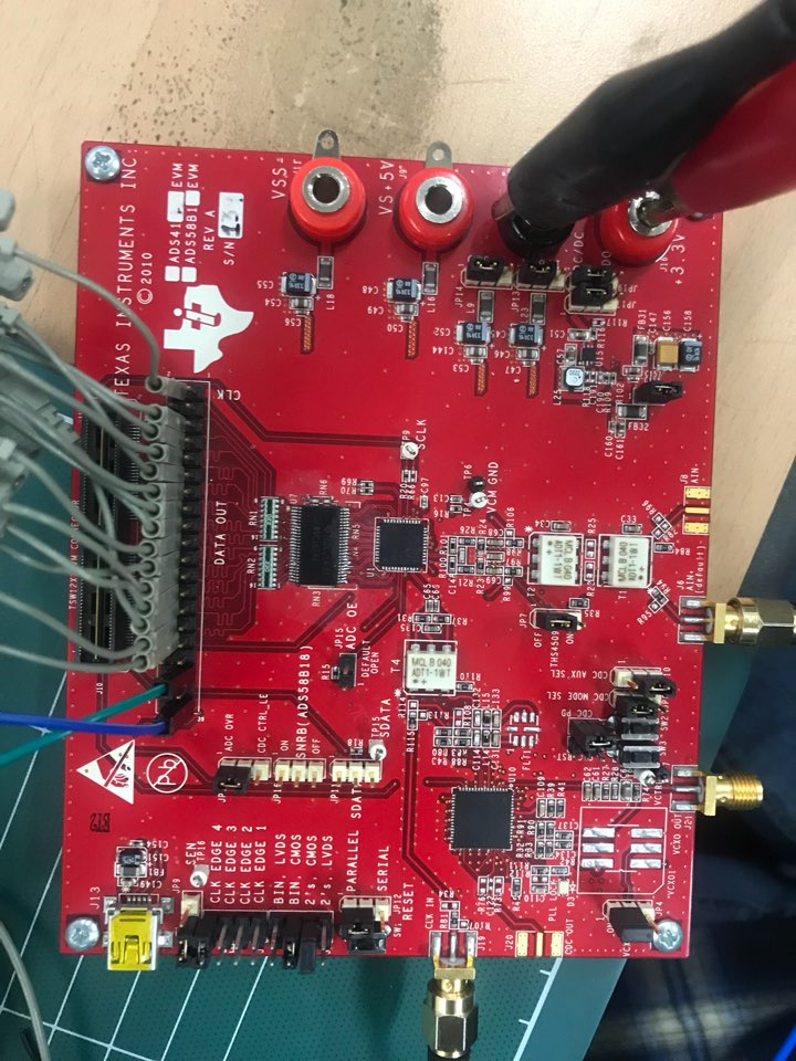
Part Number: ADS4149EVM
Other Parts Discussed in Thread: ADS4149

Hi,

Can you guys help me?

I'm using ADS4149EVM for adc.

what I'm trying to do is checking that the ads4149evm is correctly working. So I've already checked with TWS1400EVM. It means the TSW12XXEVM is working for checking output data. 

For the next stage, I've tried to check output date through MSB which is right blow TSW12XXEVM.

 BUT it isn't working at all. there are any signal.

please tell me how to use MSB , how to get a date through MSB port. 

thank you.

  • Hi Sung
    We are looking into your questions. Someone will respond soon.
    Jim B
  • Sung Young,

    Your post is very confusing. Are you using the ADC with a TSW1400EVM or a TSW1200EVM? If it is the TSW1200EVM, this board is no longer supported and you must use the TSW1400EVM. Do you have the ADC setup for serial or parallel SPI interface? If it is setup for serial SPI, how are the ADC registers configured? If setup for parallel SPI, did you press the board reset after power up? What sample rate is the ADC running at? What is the IF frequency and amplitude?

    Regards,

    Jim

  • Thank you for giving the answer.

    I'm using ADS4149EVM for adc.

    I used with TWS1400EVM for getting output data and I scceed to get a date with TWS1400EVM.
    However, what I real purpose is getting data through MSB port not through TWS1400EVM.

    So I've been controling TWS1400EVM with USB to change the mode.
    please let me know what I shoud change in SPI and Borad to setup.


    thank you.
  • Sung Young,

    If you are trying to get CMOs data out from connector J5, you must remove RN3, RN4, RN5 and RN6 and install the buffer U7. You then need to set the ADC to output CMOS data either by writing to the correct registers per the data sheet using the SPI with serial mode or by setting the jumpers per the User's Guide if using SPI parallel mode. 

    Regards,

    Jim

  • Jim

    Thank you for your answer.

    I'm trying to what you told me. I just removed RN3, RN4, RN5 and RN6 and installed the buffer U7. But I still have some problem. I can not understand how I should set the ADC to output CMOS data and else. Could you tell me more detaile about how I set the ADS4149 EVM for change the output date?

    SH3 D0_D1-P -->>> D0
    SH3 D0_D1-M -->>> D1
    SH3 D2_D3-P -->>> D2
    SH3 D2_D3-M -->>>D3
    ... -->>> ....
    (LVDS) (CMOS)

    THAT IS WHAT I REALY WANT TO GET FOR THE OUTPUT DATA.

    Sung Young,
  • Sung,

    If you are using parallel SPI mode, set the jumpers according to the User's Guide to set the part in CMOS output mode. Next, apply power and a send a clock source to J19, and then issue a rest. If using serial SPI mode, after power  and clock are present, write to the corresponding register to issue a reset then set the output to CMOS mode. Using a scope probe, verify that the data out of the ADC is toggling and is at the correct voltage level. After this, do the same test but at the buffer output. If you are still having problems, send me the jumper settings used by your board. If you are using the GUI, send screen shots of the GUI settings.

    Regards,

    Jim 

  • Thank you foryour  answer.


    Here is the biggest problem.
    At present ads4149EVM has installed a buffer on U7 and when 3.3V  for  is applied to Vcc of the buffer and 1M MAPS,
    the current was over 400mV, so I stopped the operation and lowered the Vcc of the buffer to 2V.

    I want to know how much current will flow at this condiction at 3.3V in usual.


    As a result of the measurement, it was confirmed that the data is outputted through the U7 in only LVDS mode.
    And then I use JP12 to change to SERIAL mode and J2 to change both the LVDS and CMOS modes.
    I checked the change, but the signal did not change.
     Once again, let us know the SETTING value for each PIN number of SERIAL mode and PARALLEL mode.

  • Set your jumpers as follows for parallel CMOS output mode:

    J2- shunt on pins 3-4 and 15-16

    JP9 1-2

    JP18 1-2

    JP11, JP16, JP15 no shunt

    JP12 1-2

    JP4 1-2

    JP8 1-2

    JP10 2-3

    JP7 1-2

    JP14 1-2

    JP13 1-2

    JP17 1-2

    JP19 1-2

    JP3 installed.

    This gives a CMOS output on our EVM. Press switch SW1 after power and clock is present.

    Regards,

    Jim

  • Thanks again.

    We just follow what you told me. But it didin't work.

    here are some picture which is our situation and condition.

    POWER SUPPLY USE CH2

    and I still wander how much current will folw at this EVM. 

    And here is one more thing that I confuse that you told me J2- shunt on pins 3-4 and 15-16

    but J2 has only 1 to 8.

  • Sung,

    J2 is a 20 pin connector. This is why I called out the locations as I did. You need to provide 3.3V. It appears your current limit is set to low. What is the frequency and amplitude of your clock?

    Regards,

    Jim  

  • Here is only 8 pin. isn't this correct?

    clk : 10MSPS, 1Vpp  

    INPUT: 50KHz ,1Vpp

    Thank you so much.

  • And we still get output with conplementary data.

    It is looks like this.

    Thank you.

  • Sung,

    Move the jumper from J2 from pins 3-4 to 5-6. This will change the output from CMOS 2's comp to CMOS offset binary per the silkscreen markings on the board.

    Regards,

    Jim

  • Thank you.

    we gat binary data finally.

    But the results are unsatisfactory.

    I put a sine wave into the input signal, but the result is as follows.

    and here is the contition of this result.


     that is power supply.

    and this picture shown the input and clk. the upside of picture shown

    input : 2MHz , 0.3Vpp 0v offset.

    clk : 20MHz , 1Vpp ,0V offset.

    what is the problem?

    thank you.

  • we thought that was binary code, but it wasn't. that only because delay time at 3.3V. when we change the Voltage just little , it gose back for comp.
  • Jim.

    I gat the data which is look like 2' complement data, but I'm not sure about it.
    So I want to know what is difference between offset binary data and 2' complement data.

    I want to get the offset binary data , and also I want to know how to change from 2' complement data to offset binary data.

    Thank you