This thread has been locked.

If you have a related question, please click the "Ask a related question" button in the top right corner. The newly created question will be automatically linked to this question.

ADC12DJ3200EVM: Autoset of REFCLK nebo CORECLK

Part Number: ADC12DJ3200EVM
Other Parts Discussed in Thread: ADC12DJ3200, LMK04828

Hi

I work with ADC12DJ3200  ADC and digilent board.

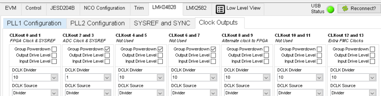
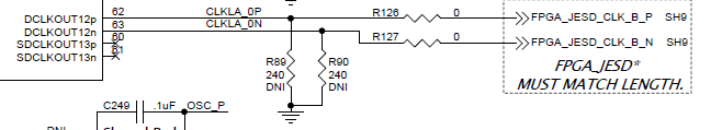
I want to reach 5 GSPS, JMODE0, so the linerate is 10 Gbps, refclk 500 MHz and coreclk is 250 MHz.

In GUI, i choose Fs = 2500 MSPS with JMODE0. I want use CLKOUT0 for refclk and clkout12 for coreclk. How can I correct setDCLK divider? I think that LMK04828 input frequency is 3.2 GHz, is it correct?

  • Hi Tomas

    When configured for JMODE0 with a clock frequency of 2500 MHz, the 2 clocks sent to the FPGA are at 250 MHz by default. The LMK04828 receives the same input clock frequency as that sent to the ADC, in this case it is 2500 MHz.

    To change one of the FPGA clocks to 500 MHz, you just need to change the appropriate DCLK Divider from 10 (A hex) to 5 (5 hex).

    The CLKout1 DCLK Divider is for FPGA_JESD_CLK_A which is sent to FMC connector pins D4 and D5. 

    The CLKout8 DCLK Divider is for FPGA_JESD_CLK_B which is sent to FMC connector pins G6 and G7.

    To permanently change these settings to work for this capture board you can edit the LMK04828 configuration file for JMODE0. The file is located in this folder location "C:\Program Files (x86)\Texas Instruments\ADC12DJxx00 GUI\Configuration Files".

    The file is named "LMK04828_JMODE0.cfg". 

    Just make a copy of the original file for backup purposes and then make the necessary edit.

    The CLKout1 DCLK Divider is at Register 0x100

    The CLKout8 DCLK Divider is at Register 0x130

    Let us know if you need anything else.

    Best regards,

    Jim B

  • Hi Jim,

    thanks for your fast response.

    "The CLKout8 DCLK Divider is for FPGA_JESD_CLK_B which is sent to FMC connector pins G6 and G7."

    But in schematic I see, that CLKOUT12 DCLK divider ii for JESD_CLK_B, is it error?

  • Hi Tomas

    You are correct. DCLKout12 is used for FPGA_JESD_CLK_B. The divider value address 0x130h I gave is correct for DCLKout12.

    I just referred to DCLKout8 by mistake. The divider for that output is at 0x120h.

    Best regards,

    Jim B

  • Jim
    Thank you for the clarification, it solved my problem.